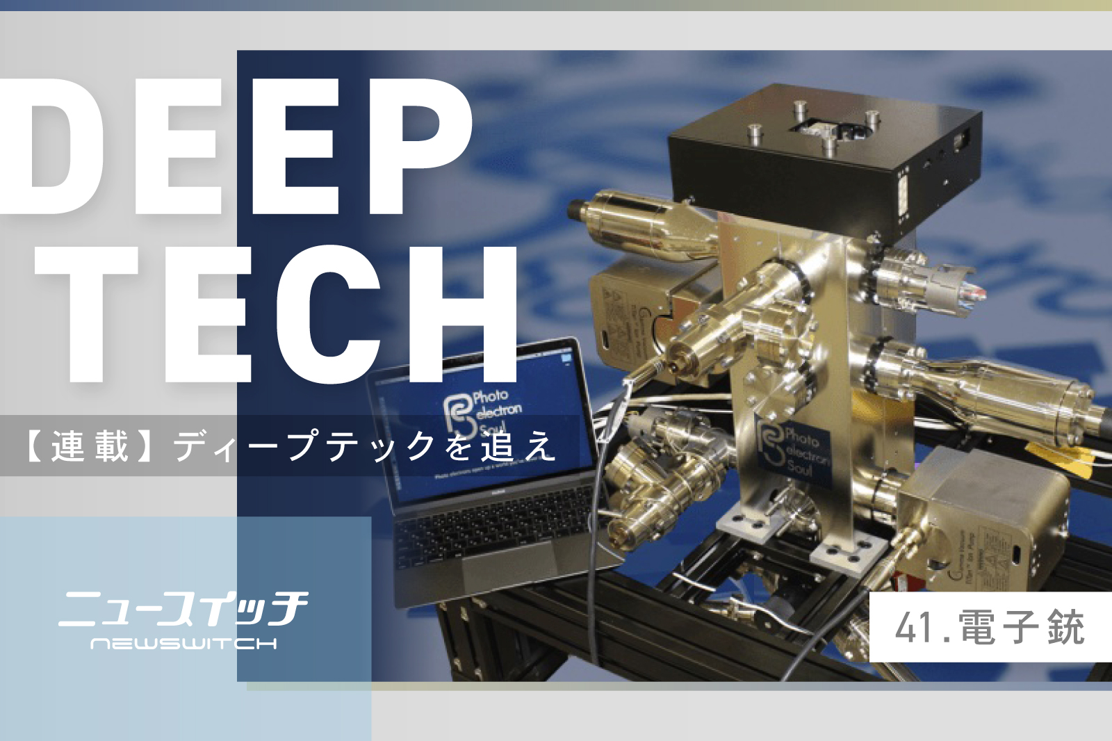
Photoelectron Soul: Miniaturization of the electron gun of a large accelerator:
-Electron gun that irradiates an electron beam-
SPring-8
Huge electron gun
A large accelerator represented by a large radiation facility (SPring-8).
The SPring-8 is equipped with a “giant electron gun that irradiates an electron beam.”
Large accelerator:
Large accelerators
Particles such as electrons and protons,
Accelerate to near the speed of light,
Create a high energy state.
It is used to “approach the origin of the universe and elucidate the three-dimensional structure of proteins.”
Nagoya University Venture
Photoelectron Soul
This large, high-power electron gun has been downsized.
The light source was downsized and revolutionized for the first time in half a century.
Aiming to develop into semiconductor inspection equipment, electron microscopes, and surface processing.
Semiconductors to be miniaturized:
The electron beam emitted from the electron gun is indispensable for nano-level processing and inspection.
In particular, the importance of semiconductors, which are becoming finer, is increasing.
The company’s focus was on the “defect inspection process for semiconductor silicon wafers.”
Pre-process of semiconductor manufacturing:
The process of inspecting “whether there is any abnormality in the silicon wafer to be filmed or exposed”.
Since “abnormalities are caused by dust, etc.”, the location of occurrence is random.
Photoelectron Soul
President Takayuki Suzuki
Current issues:
Currently, he points out that “the mainstream field emission (FE) type takes 16 hours to inspect.”
Eliminate the problem with electron guns:
“Thermionic emission type and FE type, which are the standard methods of electron guns” have weaknesses.
The point is that there is a “trade-off between the probe current applied to the sample and the size of the light source”.
Thermionic emission type:
In the thermionic emission type, the current can be increased, but the light source size is large.
Field emission (FE) type:
The FE type is the opposite, the current is small, but the light source size can be reduced to the nano level.
High resolution analysis is possible.
FE type issues:
FE type born more than 50 years ago.
It has revolutionized the ability to irradiate an electron beam with a smaller light source size than the thermionic emission type.
However, the limitations of the fine world and the time cost issues have arisen.
“Semiconductor photocathode” method:
The company uses an electron gun of the type called “semiconductor photocathode”.
Achieves efficient fine inspection:
The semiconductor photo cathode is
Using a high energy accelerator,
The properties and behavior of elementary particles and atomic nuclei,
It has been used when observing.
Miniaturized to 1/6:
To create a “Big Bang” state
The fact that it was high output and large
Until now, it has been an application issue.
The company has succeeded in reducing this to one-sixth of the conventional size.
Semiconductor material of accelerator:
In addition, the fact that the internal semiconductor that generates the electron beam deteriorates quickly has also been regarded as a problem.
Therefore, the accelerator semiconductor material was GaN.
Deterioration was suppressed and continuous use time was greatly increased.
Applied to electron microscope and metal processing:
It has become possible to emit various electron beams such as pulsed light and multi-electron beam.
In addition, the inspection time for semiconductors has been significantly reduced.
Irradiation time reduced to 1/10:
The “probe current indicating the amount of current applied to the sample” is 10 times or more higher than that of the FE method.
If it is only the irradiation time, it can be reduced to 1/10 by simple calculation.
Mass production of 10 units started annually:
In 2020, it was adopted as a part of semiconductor inspection equipment, and mass production of about 10 units has started annually.
Field of electron microscopy:
Looking ahead is the field of electron microscopy.
In the past, it was difficult to capture moving objects.
By applying the pulsed light emitted from the electron gun, we aim to continuously capture objects.
Used in battery materials and pharmaceuticals:
It is expected that it can be used for observing the movement of battery materials on the metal surface and for pharmaceutical products.
Field of metal processing:
Furthermore, we will also consider fields such as metal processing such as 3D printers.
New switch