
GaN ingot: continuous laser irradiation
ーCutting out wafers from ingotsー
-Disco’s New Wafer Detachment Technology-
We will deliver a summary from the Nikkei Cross Tech (xTECH) article.
精密加工装置メーカー:ディスコ
Precision processing equipment manufacturer: DISCO
Gallium nitride (GaN), a power semiconductor material
We have developed a new process for cutting wafers from ingots (Fig. 1).
DISCO’s new technology for separating wafers from GaN crystal ingots.

Adopt new process
Disco Japan announced on July 3, 2023, “Technology for peeling wafers quickly and without waste using a laser.”
A 2-inch (5 cm) ingot yields a 38% higher wafer yield.
The number of sheets produced per hour is improved by 6 times compared to conventional machines.
Currently in the prototype stage. We will continue development toward mass production.
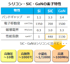
Next-generation power semiconductor material GaN:
GaN has higher physical properties than silicon carbide (SiC).
It is attracting attention as a next-generation power semiconductor material.
GaN substrates are expensive
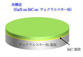
For maximum utilization, vertical GaN is required, which is a layer of GaN on a GaN substrate.
However, GaN substrates are currently more expensive than Si and SiC.
This is one of the factors that hinder the spread of vertical GaN.
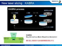
KABRA process for GaN
This time, a new process developed by DISCO.
DISCO has already applied a process called “KABRA” for SiC.
A GaN ingot is continuously irradiated with a focused laser at the desired depth of slicing.
A separation layer is provided and wafers of the desired thickness are released.
This is polished to form a wafer.

For wire saw process:
Traditionally, the cutting process uses a diamond wire saw.
A material loss occurs by a thickness equivalent to the thickness of the wire saw.
Furthermore, waviness occurs on the surface of the wafer during cutting.
Moreover, after cutting out, the surface must be largely scraped off.
For laser processing
Minimal material loss in cutting and smooth surface.
Laser processing has high throughput.
Less material loss during cutting and polishing.
https://xtech.nikkei.com/atcl/nxt/column/18/01537/0086
2023 | News | DISCO Corporation
High mass-productivity:
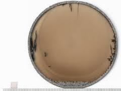
Φ4 inch GaN Wafer after separation and grinding
High throughput:
Developed a special optical system and processing method optimized for GaN
Efficient creation of KABRA layer*1 due to short stage scanning distance
High yield:
Efficiently discharges the Nitrogen that is produced within the material and prevents wafer breakage by also creating a uniform KABRA layer near the edge of the ingot

KABRA Process Flow for GaN Wafer Mass Production
Laser is irradiated inside the ingot and KABRA layer is formed
Ingot separated into wafer
Wafer ground to specified thickness
Ingot upper surface ground for next laser irradiation