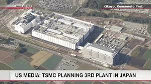
Taiwan’s TSMC: to build third factory in Japan
~ Opportunity arrives for Japanese semiconductors
~TSMC’s ‘de-dependence on China’ progresses
We will provide you with a summary of articles published on President Online.

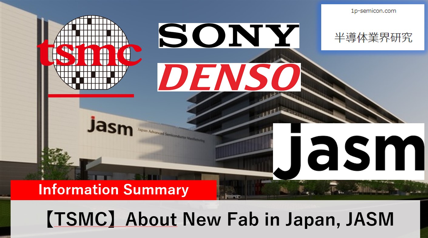
TSMC’s Kumamoto 3rd Factory:
In November of this year, it was reported that TSMC was considering building a third factory in Kumamoto.
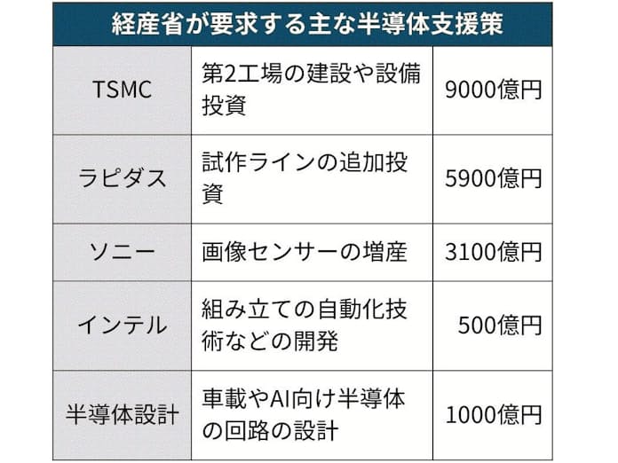
1. Accelerate expansion of production facilities in response to increased use of AI.
2. We plan to manufacture logic semiconductors with a circuit line width of 3 nm.
The investment scale is expected to reach 2.9 trillion yen. Details are not clear.
TSMC is considering building a third factory in Kumamoto in search of a more stable business environment.
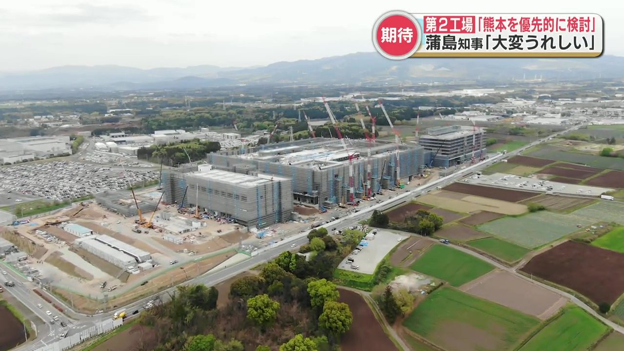
TSMC’s Kumamoto 2nd Factory:
In October of this year, TSMC announced plans to produce cutting-edge semiconductors with circuit line widths of 6 nm at its second factory in Kumamoto.
A month later, they plan to build a cutting-edge semiconductor factory with a circuit line width of 3 nanometers.
Responding to the rapid increase in AI semiconductors:
Japan’s semiconductor technology is essential for expanding the use of AI around the world.
1. Japan’s semiconductor manufacturing equipment and ultra-high purity semiconductor components fully support AI.
2. Lapidus aims to manufacture 1nm chips. Semiconductor technology has improved dramatically.
TSMC collaborates with Japan:
For TSMC, the importance of relationships with Japan’s semiconductor manufacturing equipment and related parts industries has increased.
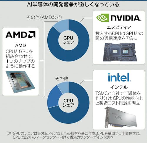
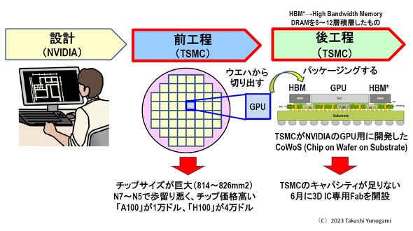
NVIDIA’s AI chip:
TSMC will use a cutting-edge semiconductor manufacturing line currently in operation in Taiwan in Japan.
It manufactures chips for AI such as Nvidia’s H100.
TSMC also announced plans to build a factory with a 3nm production line in Arizona, USA.
TSMC’s “de-dependence on China”:
Currently, Taiwan faces potential pressure from China.
TSMC and customer companies:
TSMC will promote diversification of geopolitical risks.
There is an urgent need to establish a stable chip procurement system.

Taiwan’s resource shortage problem:
In Taiwan, the rapid growth of the semiconductor industry has led to shortages of water, electricity, and human resources.
U.S. talent shortage problem:
In the United States, the start of factory operations is likely to be delayed due to soaring costs for labor and materials.
There is an urgent need to quickly resolve these issues.
TSMC’s weaknesses:
It is extremely important that AI has spread faster than expected.
1. TSMC is currently unable to keep up with global demand.
2. Meanwhile, demand for chips in cutting-edge fields such as AI is rapidly increasing.
NVIDIA and Microsoft:
Nvidia and Microsoft are designing and developing AI-compatible semiconductors in-house.
This manufacturing will be outsourced to TSMC. Therefore, supply capacity is not keeping up with demand.

TSMC’s supply capacity shortage:
The cause of TSMC’s lack of supply capacity lies at the level of semiconductor manufacturing and post-processing.
Pre-process: In the pre-process, ‘semiconductor circuits are formed on the silicon wafer’
Post-process: Polish the wafer, cut out the chips, and enclose them in a case. Perform wiring with peripheral equipment.
TSMC is weak in post-processing:
1. TSMC is the world leader in front-end processes.
2. However, TSMC’s post-process technology is still in the process of development.
Companies specializing in back-end processing in Taiwan:
In Taiwan, there are many companies specializing in back-end processing, such as Sun Moon Light Investment Holding (ASE).
However, for now, countermeasures against China risk are most important.
Semiconductor manufacturers other than TSMC:
In fact, the post-processing related processing of cutting-edge chips has not been adequately addressed.
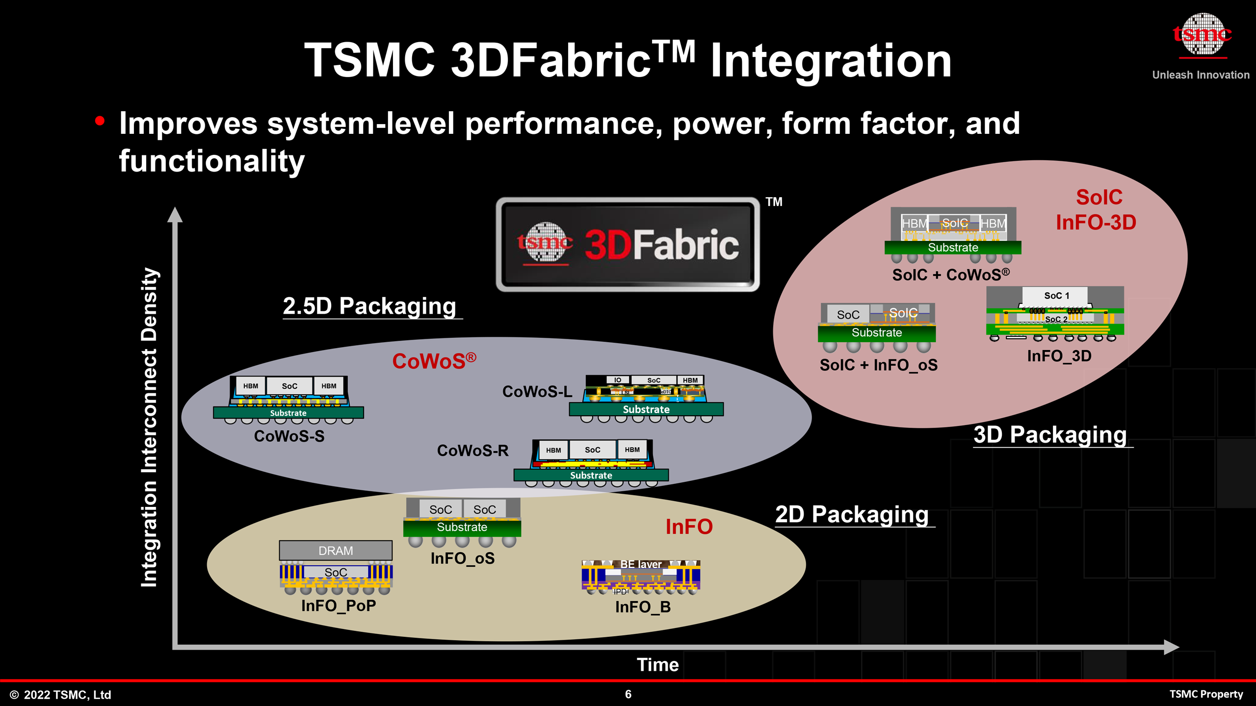
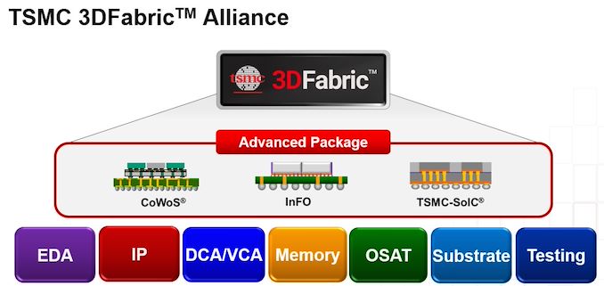
Importance of 3D semiconductor “post-process”:
Profit opportunities for Japanese companies lie in the “post-processing” of 3D semiconductors
Japanese companies have already secured a high global share in “back-end processes.”
What is 3D semiconductor post-processing?
This field includes polishing equipment for silicon wafers with circuits formed thereon, and encapsulation materials.
TSMC collaborates with related companies not only in front-end processes but also in 3D semiconductor back-end processes.
1st step: Grinding: Polish the 6nm or 3nm circuit wafer from the previous process.
Second step: Dicing: Cutting the integrated circuit from the wafer and making it into a chip.
3rd step: Die bonding: After the chip is fixed to the electronic component board, electrodes are attached.
4th step: Molding: The chip is sensitive to impact and is enclosed in a case.
Japan is a hub of suppliers:
There are also many companies with high technological capabilities in the United States, the Netherlands, and Singapore.
However, the ‘major suppliers of front-end and back-end equipment and parts’ are all concentrated in Japan.
TSMC and Japanese suppliers:
TSMC wants to further strengthen its ties with Japanese suppliers.
“Investment in Japan by Taiwanese companies specializing in back-end processes” will also increase.
TSMC’s business diversification:
Will TSMC build an automotive/semiconductor manufacturing line in Japan?
1. Strengthening collaboration with TSMC will dramatically improve the quality of semiconductor manufacturing in Japan.
2. We hope to see synergistic effects with Lapidus’ 1nm circuit linewidth semiconductors.
https://news.yahoo.co.jp/articles/0127cc1f7abecf6abba665af591e8ba52598f072