TSMC: Kumamoto Joint Venture Fab with Sony:
-Responding to production contracts from around the world-
-TSMC Chairman said-
table of contents:
Reason for making a joint venture with Sony
What is the specialty technology used in Kumamoto Fab?
TSMC:
Held financial results briefings for the fourth quarter of 2021 and the full year of 2021 held on January 13.
Q & A with a securities company:
Chairman Mark Liu:
Japan Advanced Semiconductor Manufacturing (JASM), a joint venture with Sony
The front-end process fab is a base that responds to manufacturing contracts from companies around the world, in addition to its main customer Sony.
Reasons for making a joint venture with Sony:
KGI Securities Co., Ltd.
Laura Chen’s question
Overseas expansion of TSMC:
I have a question about TSMC’s overseas expansion.
Is TSMC considering a joint venture in Europe as well as in Japan?
Or do you prefer a 100% owned business?
Answers to this question
Mark Liu (TSMC Chairman)
We are considering evaluating the expansion of our factory into Europe.
It is still in the very early stages.
First and foremost is the needs of our customers.
Japanese fab:
Japanese fabs are a joint venture under the current plan.
This joint venture in Japan is a special exceptional case.
All TSMC Fabs:
We serve all customers around the world, regardless of location.
And the same is true for Japanese joint ventures.
Utilizing Sony’s proprietary technology:
However, there is one very large customer in Japan (probably Sony Semiconductor Solutions).
Using proprietary technology (probably CMOS image sensor technology), we can leverage its factory operation and manufacturing experience.
This helps to speed up the rise of the learning curve.
We have decided to operate the fab as a joint venture with Sony.
However, we hold most of the joint venture’s share (Sony’s share is less than 20%).
Therefore, this is a special case.
We are basically 100% owned by the fab, which is wholly owned by us.
What is the specialty technology used in Kumamoto Fab?
TSMC CEO
C, C. Wei
We answered institutional investors’ questions about the 28nm process that will be applied to the Kumamoto Fab.
Long-term demand at 28nm:
CMOS image sensors and non-volatile memory
Supported by Specialty Technology.
What is Specialty Technology:
CMOS image sensor,
MEMS, non-volatile memory (flash, MRAM, ReRAM),
RF, Analog, High breakdown voltage, BCD (Bipolar CMOS / DMOS)
Specialty technology refers to the above technologies and so on.
It is different from the general-purpose logic CMOS process used in in-vehicle processors.
TECH +
https://news.mynavi.jp/techplus/article/20220117-2250537/
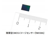
48MP sensor for iPhone 14 Pro
-Manufactured by Sony and TSMC-
-Is it produced in JASM in Japan? –
For iPhone 14 Pro
48 million pixel sensor
The iPhone 14 Pro is expected to be equipped with an effective 48-megapixel stacked CMOS image sensor for the first time.
Sony’s lack of in-house production capacity is clear.
Expand cooperation with TSMC in 2022.
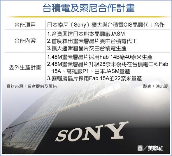
Industry and Commerce Bulletin
The Pixel Layer Chip is expected to be released to TSMC for the first time, the Industry and Commerce Bulletin reports.
Apple supply chain
Sony plans to increase foundry orders for bare-stacked CMOS image sensor components from TSMC in 2022.
48M pixel layer wafer
Manufactured on Fab 14B in Southern Taiwan using TSMC’s 40nm process.
After that, he said that he plans to upgrade and expand using a special process of 28nm.
–ITmedia NEWS
https://www.itmedia.co.jp/news/articles/2201/25/news090.html
索尼CIS元件 擴大下單台積電 – 財經要聞 – 工商時報