Photonic crystal laser: short pulse and short wavelength:
– Watt class high beam quality! Developed GaN system
stanley electric
Kyoto University
November 7th,
We have developed a “semiconductor laser using a photonic crystal as a cavity”.
Composed of GaN material:
As a result of being composed of GaN-based materials,
Achieving high beam quality with watt-class output,
Succeeded in short-pulse laser oscillation.
British scientific journal “Nature”:
Published in Communications Materials.
Conventional edge-emitting laser:
Conventional edge-emitting lasers
“Expanding the light emission area for the purpose of high output,”
There was a “problem that the beam quality deteriorated”.
again,
Since the beam shape is elliptical,
There is a need to use an optical system such as a lens,
It limited the “width of laser application.”
This photonic crystal laser:
Photonic crystal lasers can solve such problems.
Current research:
With a photonic crystal laser,
The aim was to achieve watt-class high output and high beam quality.
The three important points are:
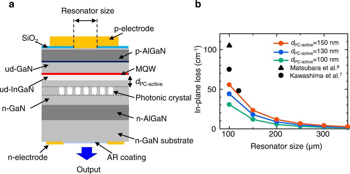
The first one:
We conducted a unique analysis of the layer structure of past devices.
It was found that “light leakage was a large value” in the in-plane direction of the device.
Sufficiently reduce in-plane loss by optimizing the layer structure and cavity size.
Second:
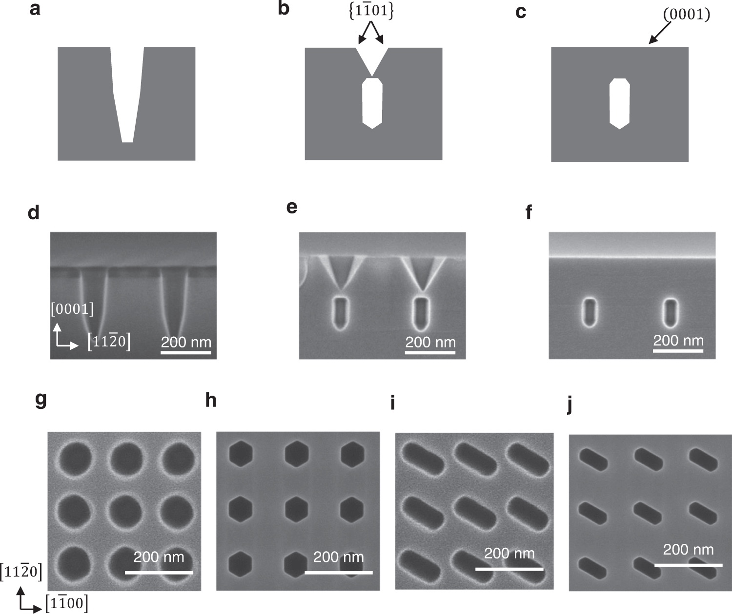
“Establishment of GaN photonic crystal formation method” and “review of photonic crystal formation method”
Conventional photonic crystal formation:
They used the “method of using an SiO2 layer as an underlay”.
With this method, the pores tend to be non-uniform,
This disturbs the resonance of the light, so
We identified the “cause of deterioration of laser characteristics”.
The conditions for the metalorganic vapor phase epitaxy method (MOVPE method) are adjusted to control the GaN crystal growth.
Developed a method to form vacancies without using SiO2.
A “very uniform, high quality photonic crystal formation” was produced.
Third:
“Employing a square lattice/double lattice photonic crystal structure”
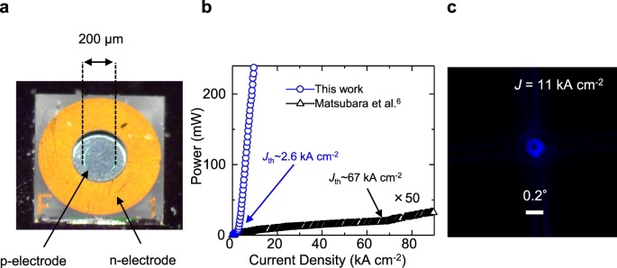
It was decided to adopt a square lattice structure that can be expected to increase output.
These 3 points:
When I made the device,
“Extremely uniform vacancy formation surrounded by crystal planes unique to GaN” was confirmed.
Power of blue wavelength:
“Watt-class output with a beam divergence of ~0.2 degrees”
Succeeded in emitting a narrow beam.
TECH+ (Tech Plus)
https://news.mynavi.jp/techplus/article/20221108-2507371/
Laser à cristal photonique : impulsion courte et courte longueur d’onde :
– Qualité des feux de route de classe Watt ! Système GaN développé
stanley électrique
Université de Kyoto
7 novembre,
Nous avons développé un “laser à semi-conducteur utilisant un cristal photonique comme cavité”.
Composé de matériau GaN :
En raison d’être composé de matériaux à base de GaN,
Atteindre une qualité de faisceau élevée avec une sortie de classe watt,
Réussite en oscillation laser à impulsions courtes.
Revue scientifique britannique “Nature”:
Publié dans Matériel de communication.
Laser conventionnel à émission latérale :
Lasers conventionnels à émission latérale
“Étendre la zone d’émission de lumière dans le but d’un rendement élevé,”
Il y avait un “problème de détérioration de la qualité du faisceau”.
encore,
Puisque la forme du faisceau est elliptique,
Il est nécessaire d’utiliser un système optique tel qu’une lentille,
Cela limitait la “largeur d’application du laser”.
Ce laser à cristal photonique :
Les lasers à cristaux photoniques peuvent résoudre ces problèmes.
Les recherches en cours:
Avec un laser à cristal photonique,
L’objectif était d’atteindre un rendement élevé de classe watt et une qualité de faisceau élevée.
Les trois points importants sont :
Le premier:
Nous avons effectué une analyse unique de la structure en couches des anciens appareils.
Il a été constaté que “la fuite de lumière était une grande valeur” dans la direction dans le plan du dispositif.
Réduisez suffisamment la perte dans le plan en optimisant la structure de la couche et la taille de la cavité.
Deuxième:
“Mise en place de la méthode de formation des cristaux photoniques GaN” et “examen de la méthode de formation des cristaux photoniques”
Formation conventionnelle de cristaux photoniques :
Ils ont utilisé la “méthode d’utilisation d’une couche de SiO2 comme sous-couche”.
Avec cette méthode, les pores ont tendance à être non uniformes,
Cela perturbe la résonance de la lumière, donc
Nous avons identifié la “cause de la détérioration des caractéristiques du laser”.
Les conditions de la méthode d’épitaxie en phase vapeur organométallique (méthode MOVPE) sont ajustées pour contrôler la croissance des cristaux de GaN.
Développement d’une méthode pour créer des postes vacants sans utiliser de SiO2.
Une “formation de cristaux photoniques de haute qualité très uniforme” a été produite.
Troisième:
“Utilisation d’une structure cristalline photonique à réseau carré/double réseau”
Il a été décidé d’adopter une structure en treillis carré dont on peut s’attendre à ce qu’elle augmente la production.
Ces 3 points :
Quand j’ai fabriqué l’appareil,
“Une formation de lacunes extrêmement uniforme entourée de plans cristallins uniques au GaN” a été confirmée.
Puissance de la longueur d’onde bleue :
“Sortie de classe Watt avec une divergence de faisceau d’environ 0,2 degrés”
A réussi à émettre un faisceau étroit.
TECH+ (Tech Plus)
Photonischer Kristalllaser: kurzer Puls und kurze Wellenlänge:
– Wattklasse Fernlichtqualität! Entwickeltes GaN-System
Stanley elektrisch
Universität Kyoto
7. November,
Wir haben einen “Halbleiterlaser mit einem photonischen Kristall als Hohlraum” entwickelt.
Bestehend aus GaN-Material:
Da es aus Materialien auf GaN-Basis besteht,
Hohe Strahlqualität mit Leistung der Wattklasse erreichen,
Erfolgreiche Kurzpuls-Laseroszillation.
Britisches Wissenschaftsjournal “Nature”:
Veröffentlicht in Kommunikationsmaterialien.
Herkömmlicher kantenemittierender Laser:
Herkömmliche kantenemittierende Laser
“Erweiterung der Lichtaustrittsfläche zwecks hoher Leistung”,
Es gab ein “Problem, dass sich die Strahlqualität verschlechterte”.
wieder,
Da die Strahlform elliptisch ist,
Es besteht die Notwendigkeit, ein optisches System wie eine Linse zu verwenden,
Es begrenzte die “Breite der Laseranwendung”.
Dieser photonische Kristalllaser:
Photonische Kristalllaser können solche Probleme lösen.
Aktuelle Forschung:
Mit einem photonischen Kristalllaser
Ziel war es, eine hohe Leistung der Wattklasse und eine hohe Strahlqualität zu erreichen.
Die drei wichtigen Punkte sind:
Der erste:
Wir haben eine einzigartige Analyse der Schichtstruktur vergangener Geräte durchgeführt.
Es wurde herausgefunden, dass “Lichtaustritt ein großer Wert” in der Richtung der Vorrichtung in der Ebene war.
Reduzieren Sie den In-Plane-Verlust ausreichend, indem Sie die Schichtstruktur und die Kavitätsgröße optimieren.
Zweite:
“Etablierung des photonischen Kristallbildungsverfahrens von GaN” und “Überprüfung des photonischen Kristallbildungsverfahrens”
Herkömmliche photonische Kristallbildung:
Sie verwendeten die “Methode, eine SiO2-Schicht als Unterlage zu verwenden”.
Bei diesem Verfahren neigen die Poren dazu, ungleichmäßig zu sein,
Dies stört die Resonanz des Lichts, also
Wir haben die „Ursache der Verschlechterung der Lasereigenschaften“ identifiziert.
Die Bedingungen für das metallorganische Dampfphasenepitaxieverfahren (MOVPE-Verfahren) werden angepasst, um das GaN-Kristallwachstum zu steuern.
Entwicklung einer Methode zur Bildung von Leerstellen ohne Verwendung von SiO2.
Es wurde eine “sehr gleichmäßige photonische Kristallformation hoher Qualität” erzeugt.
Dritte:
“Einsatz einer photonischen Kristallstruktur mit quadratischem Gitter / Doppelgitter”
Es wurde entschieden, eine quadratische Gitterstruktur zu übernehmen, die voraussichtlich die Leistung erhöhen wird.
Diese 3 Punkte:
Als ich das Gerät herstellte,
“Extrem gleichmäßige Fehlstellenbildung, umgeben von Kristallebenen, die einzigartig für GaN sind”, wurde bestätigt.
Leistung der blauen Wellenlänge:
“Leistung der Watt-Klasse bei einer Strahldivergenz von ~0,2 Grad”
Es gelang, einen schmalen Strahl zu emittieren.
TECH+ (TechPlus)
Wide-bandgap GaN-based watt-class photonic-crystal lasers
Communications Materials
Introduction
Remarkable progress
has been made in the development of high-power, broad-area, edge-emitting GaN-based semiconductor lasers,
which can emit light of blue-violet-to-green wavelengths1,2,3.
However,
the oscillation of multi-lateral modes in these lasers
significantly deteriorates their beam quality (and thus their brightness),
which limits their range of applications.
For example,
they cannot be utilized directly for the processing (cutting, melting, and deforming) of difficult-to-process materials to which their lasing wavelengths are well-matched,
such as copper and carbon fiber reinforced plastics (CFRP).
Copper is an important material
for electric cars, and CFRP is an important material for reducing the weight of cars and airplanes;
thus,
the machining of these materials with lasers is expected to contribute to future, carbon-neutral transportation.
In addition,
GaN-based semiconductor lasers can be applied to illumination including adaptive driving beam (ADB) and laser displays,
but before doing so their beam quality should be significantly improved without compromising their high output power.