NEDO:晶圓應變分佈的可視化:
-在 Mipox 的“XS-1 Sirius”中實現-
尼多
名古屋大學
米痘
6月30日
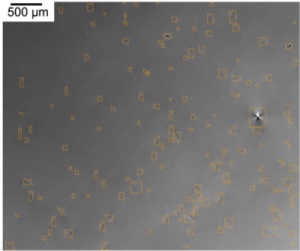
“半導體晶片內部的晶體缺陷(位錯)”以非破壞性和低成本可視化。
“殺手鐧”:
使產品的耐壓特性劣化的“殺手級缺陷”
對自動檢查“殺手級缺陷”的系統進行聯合研究。
計算位錯的系統構建和
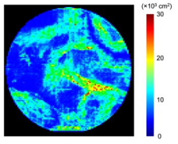
整個晶片的位錯和應變分佈
直觀、輕鬆地顯示。
成功開發熱圖顯示功能。
米痘
SiC晶體位錯
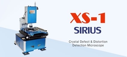
高靈敏度可視化裝置“XS-1 Sirius”
痘痘,
基於這兩項研究的結果
Mipox的產品“XS-1 Sirius”已經實現了位錯計數/熱圖顯示功能。
技術 +
https://news.mynavi.jp/techplus/article/20220701-2385564/
有助於提高半導體製造中檢查過程的便利性和效率:新聞稿 | NEDO
https://www.nedo.go.jp/news/press/AA5_101553.html
NEDO: 웨이퍼의 변형 분포를 시각화:
– Mipox의 “XS-1 Sirius”에 구현
NEDO
나고야 대학
Mipox
6월 30일,
비파괴·저비용으로, 「반도체 결정 웨이퍼 내부의 결정 결함(전위)」을 가시화했다.
“킬러 결함”:
제품의 내압 특성을 열화시키는 「킬러 결함」
「킬러 결함」을 자동 검사하는 시스템의 공동 연구를 실시.
전위를 카운트하는 시스템 구축과,
웨이퍼 전체의 전위나 변형의 분포를,
직관적으로 알기 쉽게 표시한다.
히트맵 표시 기능 개발에 성공했다.
Mipox
SiC 결정 전위
고감도 시각화 장치 「XS-1 Sirius」
Mipox,
이번 두 가지 연구 성과를 바탕으로,
전위 카운트·히트 맵 표시 기능을, Mipox의 제품 「XS-1 Sirius」에 실장했다.
TECH+
반도체 제조에서 검사 공정의 편의성 향상 및 효율화에 기여 : 보도 자료 | NEDO
NEDO: Visualisatie van de verdeling van de wafelrek:
-Geïmplementeerd in Mipox’s “XS-1 Sirius”-
NEDO
Universiteit van Nagoya
Mipox
30 juni
“Kristaldefecten (dislocaties) in halfgeleiderkristalwafels” werden gevisualiseerd met niet-destructieve en lage kosten.
“Killer defect”:
“Killer-defect” dat de weerstandsspanningskarakteristieken van producten verslechtert
Gezamenlijk onderzoek gedaan naar een systeem dat automatisch “killer defects” inspecteert.
Systeemconstructie om dislocaties te tellen en
Dislocatie en spanningsverdeling over de wafel
Intuïtief en eenvoudig weergeven.
Het is gelukt om een functie voor het weergeven van een warmtekaart te ontwikkelen.
Mipox
SiC kristal dislocatie
Hooggevoelig visualisatieapparaat “XS-1 Sirius”
Mipox,
Op basis van de resultaten van deze twee onderzoeken
De dislocatietelling / warmtekaartweergavefunctie is geïmplementeerd in het product “XS-1 Sirius” van Mipox.
TECH +
Draagt bij aan het verbeteren van het gemak en de efficiëntie van inspectieprocessen in de productie van halfgeleiders: Persbericht | NEDO
Design of automatic detection algorithm for dislocation contrasts in birefringence images of SiC wafers
– IOPscience
Abstract
Birefringence imaging
is one of the powerful methods for non-destructive characterization of defects in the semiconductor crystals.
However, due to the complicated and unclear contrasts of dislocations in the birefringence image,
it was considered to be difficult to automatically detect the position of the dislocation contrasts by the conventional image processing.
In the present study,
we designed the automatic detection algorithm for the dislocation contrasts taking into account the characteristic feature of the dislocation contrasts, which were always pair of black and white contrasts.
To detect the large change in the contrast level near the dislocation contrast,
the automatic detection algorithm
was constructed by using a variance filter.
Finally,
we succeeded in detecting the position of the dislocation contrasts with relatively high precision and sensitivity.
https://iopscience.iop.org/article/10.35848/1347-4065/abde29/meta