
China’s advanced technology: Rapid evolution of semiconductor performance
・Many Chinese-made equipment at famous universities
・Promote research with ‘211 process and 985 process’
We bring you a summary of articles published in Nikkei Crosstech (xTECH).
China’s semiconductor development:
China aims to increase the domestic production ratio of semiconductors.
Naturally, China is putting a lot of effort into “semiconductor education.”
In fact, there is a large demand for human resources from the Chinese semiconductor industry.
Visit to University of Electronic Science and Technology of China: (Photo 1)
In December 2023, the author visited Chengdu City, Sichuan Province.
Visited the University of Electronic Science and Technology, which provides graduate level semiconductor education.
China’s semiconductor education policy
The Chinese government will strengthen research and education related to semiconductors.
Established ‘National Integrated Circuit Industry-Academia Fusion Innovation Platform’.
Top-notch 1st and 2nd school schools:
First school in 2019:
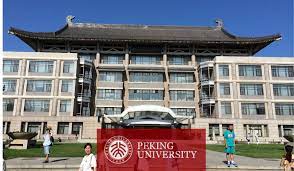
Four schools were selected for the first phase: Peking University, Tsinghua University, Fudan University, and Xiamen University.

2nd term school in 2021:
Four schools were selected for the second phase: Huazhong University of Science and Technology, Nanjing University, University of Electronic Science and Technology, and Xi’an University of Electronic Science and Technology.
It is a top-notch university where less than the top 1% of Chinese high school students enroll.

‘211 process and 985 process’ program
The above universities were selected for the 211st and 985th processes of the China Priority Program.
Currently, it has been certified as a “two-tiered” integrated program.
1. 1st period school:
Tsinghua University and Peking University are located in the Bohai Rim region.
Fudan University is located in the Yangtze River Delta region.
Xiamen University is located in the Pearl River Delta region.
2. 2nd period school:
It covers major metropolitan areas in inland China.
Huazhong University of Science and Technology = Wuhan City,
Nanjing University = Nanjing City,
University of Electronic Science and Technology = Chengdu,
Xi’an University of Electronic Science and Technology = Xi’an City,

University of Electronic Science and Technology:
In 2021, the University of Electronic Science and Technology received a grant of 350 million yuan (7 billion yen).
We will advance research on integrated circuits through an industry-academia fusion platform.
1. At Chengdu High-tech Park (Chengdu High-tech Industrial Opening Area),
2. At Chongqing Xiyong Electronics (Chongqing Xiyongwei Electronics Industrial Park),
3. Joint research with China Electronics Technology Corporation (CETC) and others.

China Electronic Technology Corporation: (CETC)
It has a number of research institutes (Number Research Institute) under the direct control of China’s Ministry of Information Industry.
1. CETC’s research focuses on electronics and IT in general.
2. It was also designated on the US Entity List.
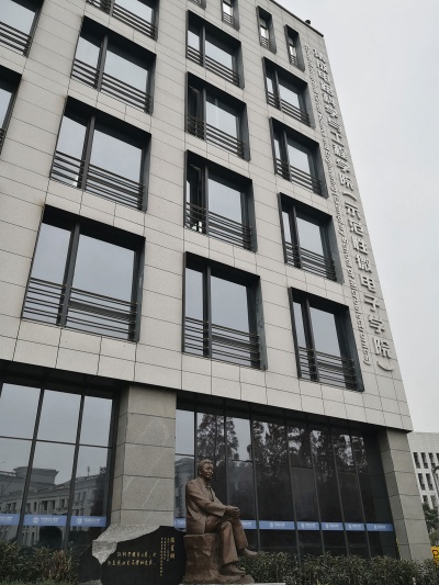
Visit to the University of Electronic Science and Technology clean room:
The University of Electronic Science and Technology has built a new building for the Department of Integrated Circuit Science and Engineering.
A bronze statue of Chen Xingbi was installed in front of the new school building.
Mr. Chen Xingbi is an accomplished person in power semiconductor research.
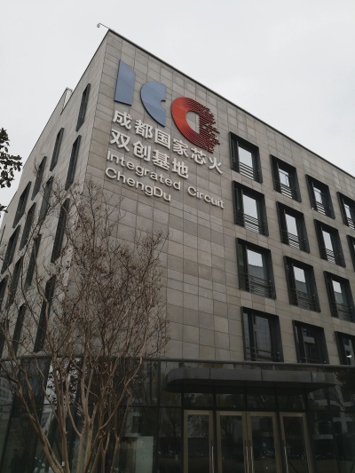
Chengdu national “core fire” Shuangzhu base:
There is also an incubation base and a Sosou base (Photo 4).
1. This is an integrated circuit design site for semiconductor companies.
2. tape out, testing, training,
3. Provide funding, incubation, etc.

Set up a clean room:
There are clean rooms on the first and second floors of the new school building.
Its size is approximately 2500m2.
In addition, there is a clean room of approximately 1000m2 that has been there for some time.
Tour the state-of-the-art clean room:
We were able to tour the latest clean room courtesy of the University of Electronic Science and Technology.
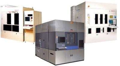
A large amount of Chinese-made semiconductor manufacturing equipment is installed there.
What stood out was the aforementioned device manufactured by China Electronics Technology Corporation.

“SEMICORE” brand:
The product has not yet been installed in a clean room. It arrived in a large container.
1. There was a wet station, dicer, grinder, etc.
2. Furthermore, the ion implantation equipment is also manufactured by the same company.
This ion implanter was only put into practical use in 2023.
Lithography equipment and etching equipment:
On the other hand, lithography equipment and etching equipment are mainly manufactured overseas.
Lithography equipment:
Japanese Nikon stepper (or scanner),
Electron beam lithography equipment from Raith, Germany
Mask aligners from Germany’s SUSS MicroTec, etc.
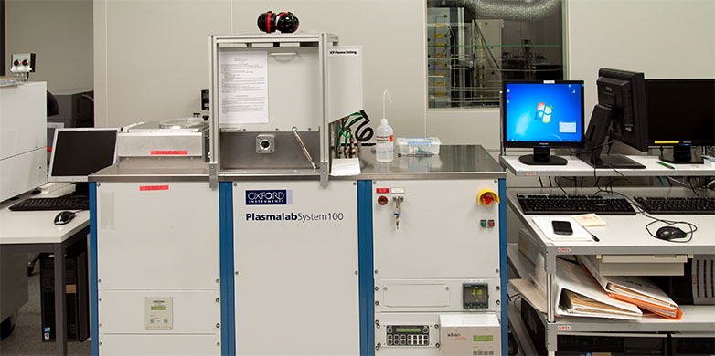
Etching equipment:
ICP (Inductively Coupled Plasma) etcher from Oxford Instruments,
Coupled Plasma etcher,
US PECVD (Plasma Enhanced Chemical Vapor Deposition) equipment,
DRIE (Deep Reactive Ion Etching) device from Korea GigaLane,

28 nm node compatible:
Front-end equipment basically supports the 28 nm node.
The exposure device appears to be a KrF stepper (or scanner).
Other than front-end equipment:
Introduced mass production mounting equipment made in China, including dicers, testers, and chip handlers.
Equipment for education and training:
Four type oxidation furnaces (3 inch, 4 inch) are installed.
It is said to be an educational device for undergraduate students to operate and practice on their own.
https://xtech.nikkei.com/atcl/nxt/column/18/00001/08905/
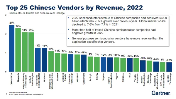
Chinese semiconductors: further expanding market share even under US regulations
We bring you a summary of articles published in Nikkei Crosstech (xTECH).
Taiwanese research company: Trendforce
We analyzed the impact of US regulations on Chinese semiconductors and mature processes.
The company predicted that China’s semiconductor and global market share will expand in the future.

China’s wafer production capacity:
China’s share in terms of 12-inch (300mm) wafers.
Production is expected to increase by 2pt from 2022 to 26% in 2026.
China share in 2026:
Estimated on the assumption that export of 40/28nm manufacturing equipment to China is approved.
China’s share in 2026 will reach 28%.
The United States, Japan, and the Netherlands implement export restrictions to China:
Restrictions on exports of semiconductor manufacturing equipment to China are progressing in the United States, Japan, and Europe.
Export restrictions on exposure equipment:
In June 2023, additional export control regulations for advanced semiconductor manufacturing equipment began in September.
In addition to EUV exposure equipment, DUV exposure equipment has been subject to export restrictions.

Impact on maturation process (55/40/28nm):
Trend force prediction:
With 55/40/28nm mature processes, there will be little impact on China’s production and development.
With the exception of photolithography-related equipment, this will be kept to a minimum.
For example, demand in China can be met by supplying film deposition equipment from Chinese companies.