台積電、英特爾、三星:只靠日本!
・我們一定要日本的後處理技術
・開始熊本、筑波、橫濱的共同研究
我們為您帶來日經 xTECH 發表的文章摘要。
半導體產業三大巨頭:
1. 台灣積體電路製造有限公司(台積電)
2. 韓國三星電子
3. 英特爾
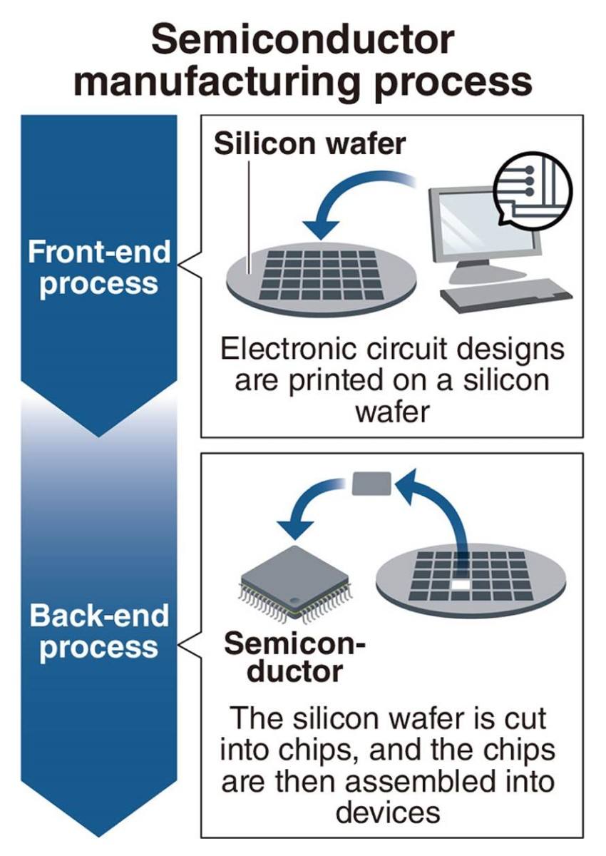
在日本建立半導體後道製程(封裝)研發基地。
我們正在加強與日本零件和設備製造商的合作。
For generative AI (artificial intelligence):
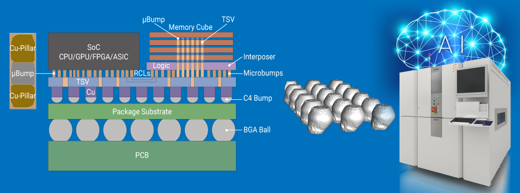
The reason behind this is the “increasing importance of Advanced Packaging.”
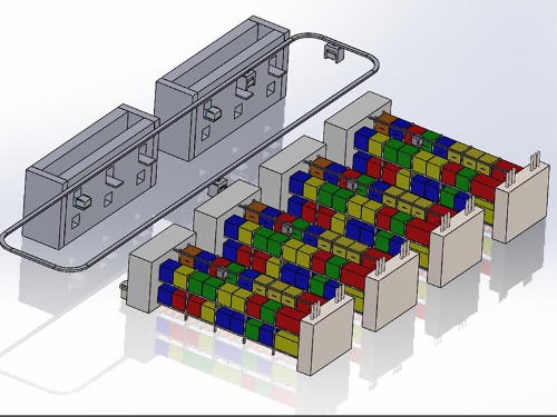
1. I want technology such as 2.5D/3D mounting.
2. It combines multiple semiconductor chips.
Japan’s high level of technology and excellent human resources attract major companies to Japan.
There will also be a move to build mass production factories for post-processing in Japan.
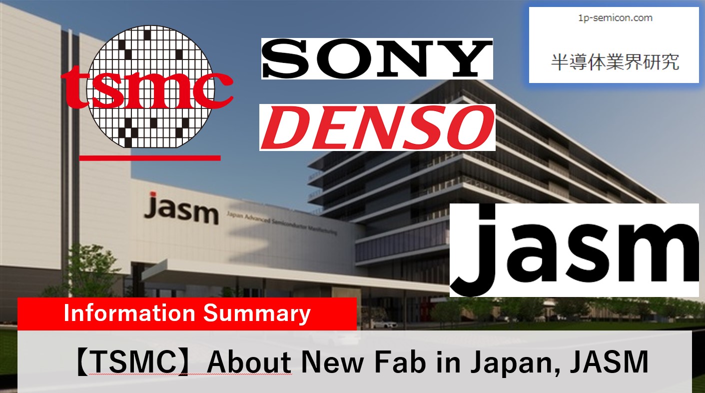
TSMC trends:
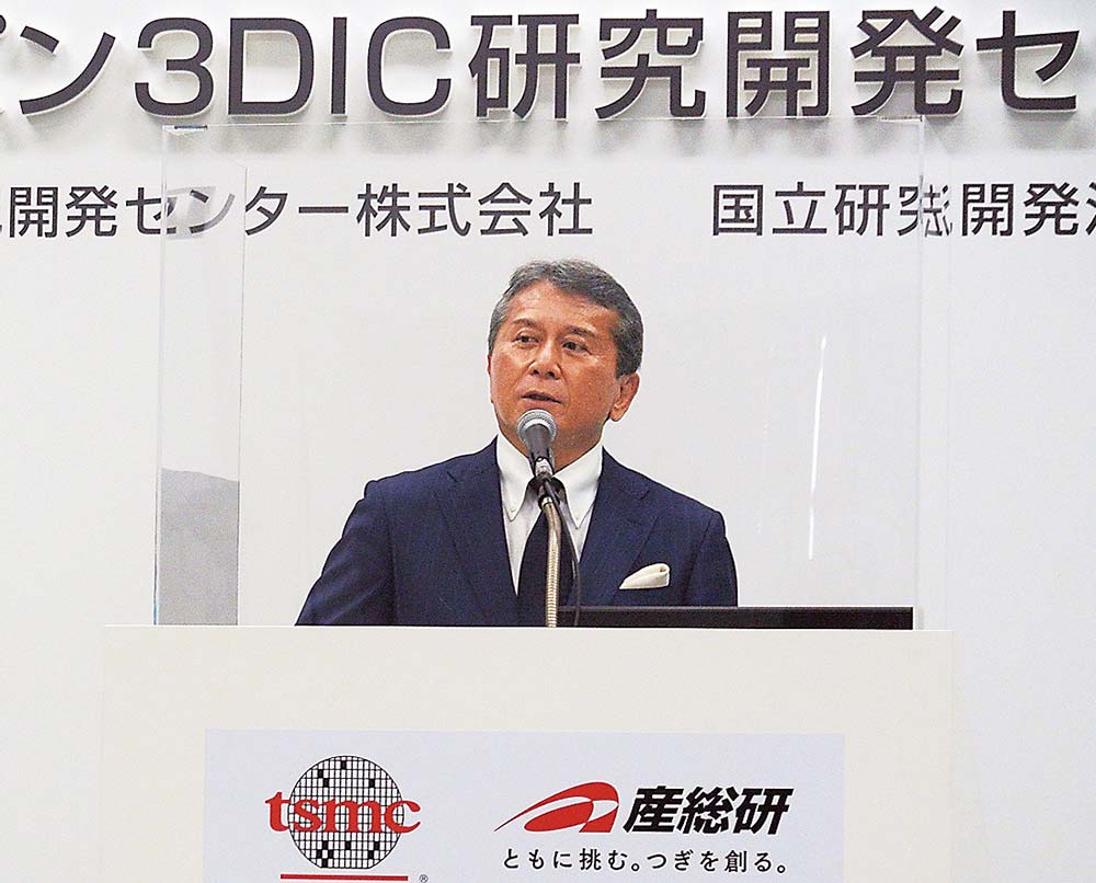
In 2022, the “TSMC Japan 3DIC Research and Development Center” was established in Tsukuba City.
1. This is the first time that TSMC has set up a development base for this technology outside of Taiwan.
2. Inquiries for US NVIDIA image processing semiconductors (GPUs) are rapidly increasing.
3. Jointly developing next-generation packaging technology in Japan.
We are currently developing 2.5-dimensional mounting technology CoWoS (Chip on Wafer on Substrate).
TSMC is also considering building a post-processing factory in Japan.
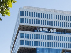
Samsung Electronics trends:
By March 2025, an advanced packaging technology and development base will be established in Yokohama.
Intel’s goals:
Aiming for ‘complete automation of semiconductor back-end processing’ in April 2024.
Joint project (SATAS):
We have launched a joint project (SATAS) with 14 Japanese equipment and parts companies.
Japanese technology is essential for the complete automation of semiconductor back-end processing.
Ministry of Economy, Trade and Industry of Japan:
Japan holds a 30% global market share in semiconductor manufacturing equipment and a 50% global market share in major components.
Japanese back-end equipment manufacturers:
1. Leading manufacturing equipment: DISCO, Tokyo Seimitsu, Yamaha Motor, etc.
2. Leading parts and products: Resonac, IBIDEN, Shinko Electric Industries, etc.
Commerce and Information Policy Bureau: Mr. Hideji Shimizu
In Japan, there are many highly skilled engineers involved in post-process development.
1. In the future, advanced packaging technology will be at the center of global semiconductor competition.
2. Supporting foundries such as TSMC and Intel in expanding into Japan.
Attracting back-end process development and mass production factories to Japan will help strengthen the competitiveness of equipment manufacturers.
https://xtech.nikkei.com/atcl/nxt/column/18/00001/09253/
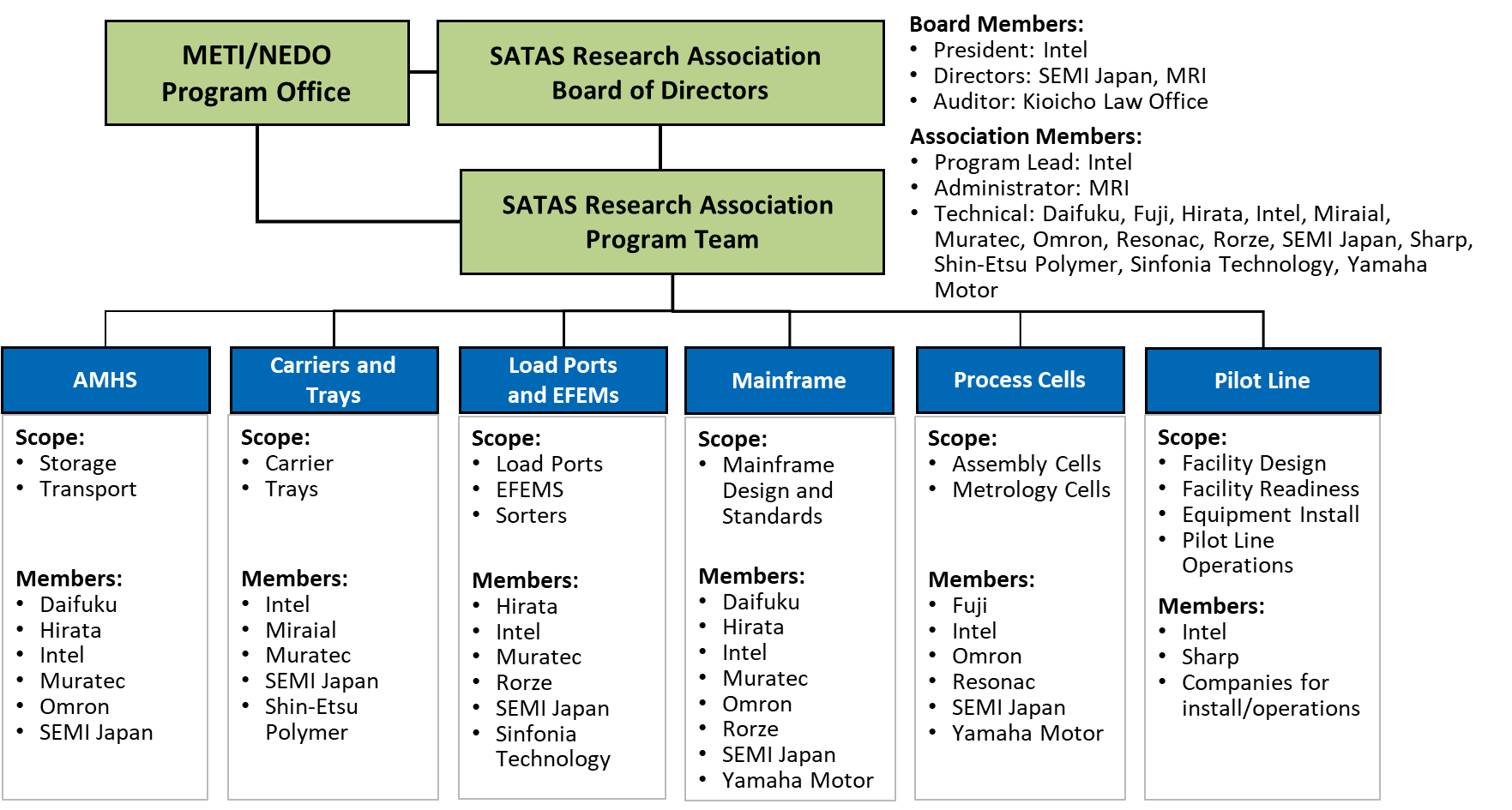
SATAS: A new organization for semiconductor back-end processing is born
We bring you a summary of articles published in Dempa Shimbun digital.
US Intel’s Japanese subsidiary:
The Semiconductor Back-end Process Automation and Standardization Technology Research Association (SATAS) was established with 14 domestic companies including OMRON.
The company aims to fully automate semiconductor packaging and assembly and testing processes.
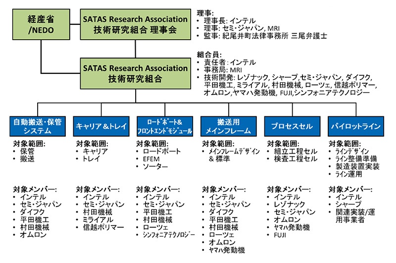
SATAS Chairman: Intel President Suzuki
SATAS was established on April 16th.
Semiconductor manufacturers, semiconductor manufacturing equipment and automatic transport equipment manufacturers will participate.
1. Development of technology necessary for automation of post-processes
2. Creation of open industry standard specifications
3. Develop and implement equipment, and verify equipment operation on the pilot line.
The plan is to introduce and implement the knowledge and technology gained.
Aiming for practical application in 2028:
1. Semiconductors are classified as “specified important materials” under the Economic Security Promotion Act.
2. In light of geopolitical risks, we will strengthen our supply chain in Japan.
Develop advanced packaging technologies such as AI.
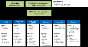
Participating companies in SATAS:
In addition to Intel, Omron, Sharp, Shin-Etsu Polymer, Symphonia Technology, Semi Japan, Daifuku, Hirata Corporation, FUJI, Mitsubishi Research Institute, Miraial, Murata Machinery, Yamaha Motor, Resonac Holdings, and Rhotse.
SATAS development system:
1. Automatic transport/storage system
2. carrier & tray
3. 6 research themes including load board & front end module
As a member, we work on development in the fields that our members are good at.
Participating company: OMRON
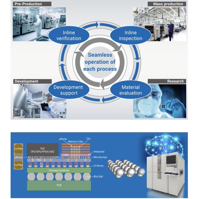
Utilizes the VT-X950 automatic X-ray inspection system for cutting-edge semiconductors announced in 2023.
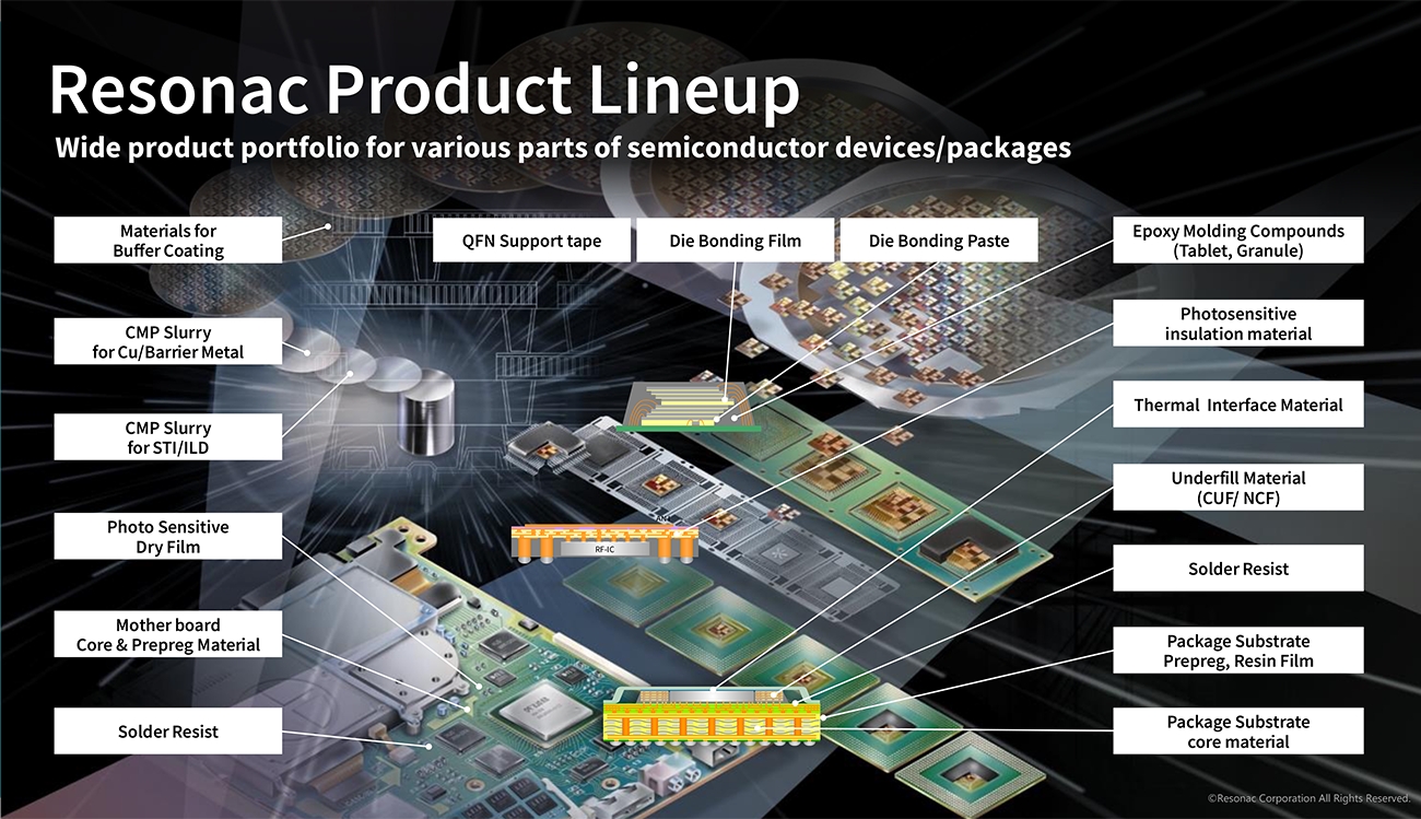
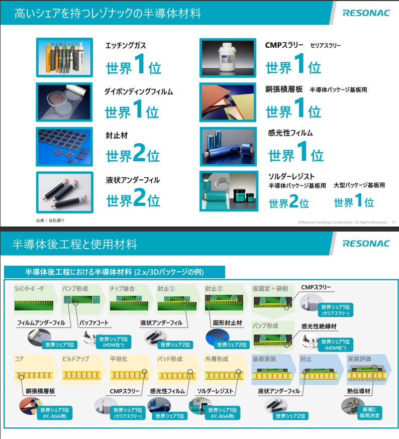
Participating company: Resonac
Utilizing the know-how of the Packaging Solution Center (Kawasaki City).
Contributes to ‘process development for assembly and inspection processes.’
https://news.yahoo.co.jp/articles/ee1279fe2d61f07bb3f499e52efde6e2be1b316c