Gigaphoton:大规模生产ArFi光源GT66A:EUV的小型化
-新技术加速技术转移-
2020年12月16日
Gigaphoton:
2020年12月16日,半导体光刻用光源制造商Gigaphoton(总部:To木县小山市,总裁:浦中克澄)
采用新技术的最新半导体制造ArF浸没式光刻光源“ GT66A”
宣布开始批量出货。
最先进的设备制造:
目前在逻辑设备中
3nm节点工艺开发开始,
DRAM已开始批量生产1Znm节点。
对于超细器件,减小转移到晶片上的曝光图案的粗糙度是一个问题。
“忠实地复制电路图形并提高批量生产的产量”是最重要的问题。
新的ArF浸入式光源“ GT66A”:
新开发的光模块。
成功地“将脉冲发射时间延长了三倍以上”
在暴露的表面上实现改善的光束均匀性。
我们成功地减少了粗糙度。
认证为ASML光源:
此外,最新的耐用组件可以将模块维护周期延长30%。
GT66A已被荷兰主要公司ASML认证为最新ArF浸没曝光设备NXT:2050i的光源。
将开始为最终用户批量生产光源。
欢迎来到Gigaphoton
https://www.gigaphoton.com/ja/news/6618
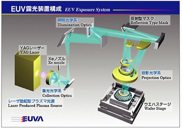
EUV曝光设备的基本配置:在图中说明
该图显示了EUV曝光设备的基本配置。
对于EUV功能模块:
激光激发型等离子光源(以下简称光源),
照明光学系统
反光罩
投影光学系统
有一个晶圆阶段。
US Cymer制造的光源:
目前,ASML的子公司Cymer生产光源。
美国政府出口审查:
由于美国政府对荷兰政府施加的压力,ASML无法将EUV运送到中芯国际。
原因之一是“ Cymer是一家在美国注册的公司,制造的光源是EUV的非常重要的模块。”
ASML将来将无法向“ SMIC”输出“使用Cymer制造的光源的EUV”。
日本生产千兆光子的光源:
但是,还有另一家可以生产EUV光源的公司。
它是日本的十亿光子。
目前,台积电和三星正在申请批量生产7至5 nm的EUV配备了Cymer制造的光源,而不是Gigaphoton。
“预脉冲”技术的起源:
也可以想到用“来自Cymer的Gigaphoton”代替ASML的EUV光源。
这是因为“ Cymer的”预脉冲“用于紫外线光源的技术”最初是“由Gigaphoton开发的”。
“预脉冲”是一种利用激光分两阶段照射锡滴的技术。
从美国Cymer到日本Gigaphoton替换EUV光源将使ASML将EUV出口到SMIC。
JBpress(日本商业出版社)
https://jbpress.ismedia.jp/articles/-/63474
NEDO:EUV试点光源展示了世界上最高的5%发射效率水平
-在NEDO项目中-
Gigaphoton Co.,Ltd .:
我们已经完成了用于EUV扫描仪的激光产生的等离子光源,该光源旨在在最先进的半导体生产线上运行。
我们已经证明了其稳定的运行性能,其输出功率为105W,发光效率为5%,这是世界上最高的水平。
随着这次操作演示的成功,我们非常接近实现最先进的半导体生产线。
尼多
https://www.nedo.go.jp/news/press/AA5_100659.html
Gigaphoton Begins Mass Production and Shipment of the ARFi GT66A Light Source Compatible with Cutting-Edge Miniaturization Technologies
December 16, 2020
Equipped with New Technologies to Accelerate a Technological Shift
Oyama, Tochigi; December 16, 2020, GIGAPHOTON Inc. (Head office: Oyama, Tochigi; President & CEO: Katsumi Uranaka), a manufacturer of light sources for semiconductor lithography,
has announced the start of mass production and shipment of the ArF immersion “GT66A” light source using new technologies for state-of-the-art semiconductor lithography manufacturing.
GT66A is now certified as a light source for the latest ARF immersion lithography equipment NXT:2050i by ASML, the leading Dutch company,
and mass production and shipment of the light source to end-users will now commence.
Leading-edge device manufacturing
has now begun with the process development of 3 nm nodes for logic devices and mass production of 1 Znm DRAM.
the yield in mass production
For these ultra-fine devices, reducing the roughness of the exposure patterns transferred to wafers is a challenge.
It is important to reproduce the circuit pattern precisely and increase the yield in mass production.
The new ArF immersion “GT66A” light source
is equipped with a newly developed optical module that successfully improves the beam uniformity on the exposed surface and reduces the roughness by increasing the temporal coherence length by at least 3 times that of the existing model.
The maintenance cycle of the module
has been extended by 30% with the introduction of the latest components with high durability.
Katsumi Uranaka, President and CEO of GIGAPHOTON, said:
“In recent years, semiconductor chips are required to support even faster communication speeds and process larger amounts of data.
This is mainly supported by the miniaturization of logic and memory semiconductors and requires higher productivity through further innovation of lithography technology.
GIGAPHOTON
will continue its contribution to the development of the next generation of industries by improving the imaging performance through technological innovation and increasing the availability of light sources.”
Welcome to Gigaphoton