ASML/尼康退出:中國的中芯國際沒有出事!
ー未來只有日本會遭受重大損失ー
香港媒體
《亞洲時報》
即使ASML、尼康退出中國市場,
“中國最大的半導體製造商芯芯國際集成電路製造(中芯國際)”是沒有問題的。
中芯國際:
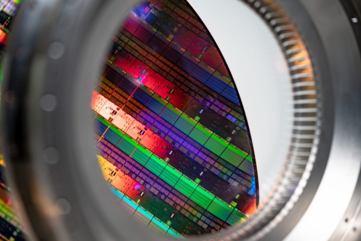
從 2022 年夏天開始,它就開始使用 7nm 工藝技術製造半導體。
這是,
7nm工藝半導體離不開ASML和尼康的半導體製造設備。
“中芯國際從阿斯麥和尼康采購了很多設備。”
“半分析”
迪倫·帕特爾
“中芯國際的產能規模”值得一看。
中芯國際已經是只用現有設備,採用7nm工藝,
有可能“每月生產100,000個半導體”。
中芯國際產能:
這“超過了三星和英特爾的總產能”。
帕特爾評論道:
如果中芯國際使用所有中國企業擁有的半導體製造設備,
中芯國際7納米製程半導體製造能力遠超台積電。
此外,在大規模生產方面,中國正在推進半導體製造設備的開發。
上海微電子設備有限公司(SMEE):
“我們已經開發出一種可以處理高達 14 納米的光刻系統,”他說。
未來中國廠商的技術也會提升。
– 雅虎新聞
https://news.yahoo.co.jp/articles/214f1f0709bf201ec2bff1b5e3916af9810d9376
ASML/Nikon se retire : le SMIC chinois n’est pas en difficulté !
ーÀ l’avenir, seul le Japon subira de grosses pertesー
médias de hong kong
“L’heure de l’Asie”
Même si ASML et Nikon se retirent du marché chinois,
“Le plus grand fabricant chinois de semi-conducteurs Core Core International Integrated Circuit Manufacturing (SMIC)” n’est pas un problème.
SMIC :
Dès l’été 2022, elle fabrique des semi-conducteurs en utilisant la technologie de procédé 7 nm.
c’est,
Les semi-conducteurs de processus 7 nm ne peuvent pas être fabriqués sans l’ASML et l’équipement de fabrication de semi-conducteurs de Nikon.
“SMIC a acheté beaucoup d’équipements auprès d’ASML et de Nikon.”
“Semi-analyse”
Dylan Patel
“La taille de la capacité de production du SMIC” est quelque chose à voir.
SMIC n’utilise déjà que des équipements existants, utilisant le procédé 7nm,
Il est possible de “produire 100 000 semi-conducteurs par mois”.
Capacité de production du SMIC :
C’est “plus que la capacité de production combinée de Samsung et d’Intel”.
Patel a commenté :
Si le SMIC utilise tous les équipements de fabrication de semi-conducteurs appartenant à des entreprises chinoises,
La capacité de fabrication de semi-conducteurs de procédé 7 nm de SMIC dépasse de loin celle de TSMC de Taiwan.
De plus, concernant la production de masse, le développement d’équipements de fabrication de semi-conducteurs progresse en Chine.
Shanghai Micro Electronic Equipment Co., Ltd. (SMEE) :
“Nous avons développé un système de lithographie qui peut gérer jusqu’à 14 nanomètres”, a-t-il déclaré.
La technologie des fabricants chinois s’améliorera également à l’avenir.
– Actualités Yahoo!
ASML/Nikon zieht sich zurück: Chinas SMIC ist nicht in Schwierigkeiten!
ーIn Zukunft wird nur Japan große Verluste erleidenー
Hongkonger Medien
“Asienzeit”
Auch wenn sich ASML und Nikon vom chinesischen Markt zurückziehen,
“Chinas größter Halbleiterhersteller Core Core International Integrated Circuit Manufacturing (SMIC)” ist kein Problem.
SMIC:
Bereits seit Sommer 2022 fertigt es Halbleiter in 7-nm-Prozesstechnologie.
das ist,
7-nm-Prozesshalbleiter können nicht ohne ASML und Nikons Halbleiterfertigungsanlagen hergestellt werden.
“SMIC kaufte viele Geräte von ASML und Nikon.”
“Halbanalyse”
Dylan Patel
„Die Größe der Produktionskapazität von SMIC“ kann sich sehen lassen.
SMIC verwendet bereits nur vorhandene Geräte im 7-nm-Prozess,
Es sei möglich, “100.000 Halbleiter pro Monat zu produzieren”.
Produktionskapazität von SMIC:
Das sei „mehr als die gemeinsame Produktionskapazität von Samsung und Intel“.
Pattel kommentierte:
Wenn SMIC alle Halbleiterherstellungsanlagen verwendet, die chinesischen Unternehmen gehören,
Die Fertigungskapazität von SMIC im 7-nm-Prozess für Halbleiter übertrifft die von Taiwans TSMC bei weitem.
Darüber hinaus schreitet die Entwicklung von Halbleiterfertigungsanlagen in China in Bezug auf die Massenproduktion voran.
Shanghai Micro Electronic Equipment Co., Ltd. (SMEE):
“Wir haben ein Lithografiesystem entwickelt, das bis zu 14 Nanometer verarbeiten kann”, sagte er.
Auch die Technik der chinesischen Hersteller wird sich in Zukunft verbessern.
– Yahoo Nachrichten
US, Japan and Netherlands in a squishy China chip ban
– Asia Times
The Wall Street Journal reported that
ASML of the Netherlands and Nikon of Japan would stop exporting “at least some immersion lithography machines” to China.
Immersion lithography means
DUV (deep ultra-violet) ArF (argon fluoride) laser lithography systems
in which the space between the final lens and the surface of the silicon wafer is filled with purified water.
Because purified water has a refractive index of 1.44 (compared with 1.0 for air),
this increases the resolution of the optics, facilitating the creation of smaller chip feature sizes.
At present, ASML and Nikon
are the only companies able to mass-produce these semiconductor-making machines.
Stopping shipments of ArF immersion lithography systems
would make it difficult for China to add new production capacity at or below the 40-nanometer node
– i.e., for the bulk of semiconductor production by value –
particularly at the 28nm and smaller nodes now used to produce
integrated circuits for automotive,
the Internet of Things,
consumer electronics,
mobile phones,
high-speed networking and computer applications.
The practical limit of DUV is 7nm.
The leading-edge 5nm and 3nm processes now in production at Taiwan’s TSMC and South Korea’s Samsung,
the 2nm processes they both have under development, rely on EUV (extreme ultra-violet) lithography systems.
These are made only by ASML and, at the request of the US government, not exported to China.
The semiconductor industry was surprised and US government officials were shocked
when it was reported last summer that China’s leading semiconductor foundry,
SMIC, had managed to produce chips using 7nm process technology.
Almost certainly, analysts say, this was accomplished by using ASML or Nikon equipment.
How many immersion lithography systems China has already purchased from ASML and Nikon is unclear,
but analysts’ estimates range from “many” to “dozens.”
Dylan Patel of SemiAnalysis reports that
SMIC, China’s leading foundry, “could achieve a capacity of well over 100,000 wafers a month of 7nm foundry capacity with their existing DUV tools alone.
This is higher than Samsung and Intel’s advanced node (<=7nm) foundry capacity, combined.”
“If all DUV tools at various Chinese nationals such as HuaHong, Shanghai Huali, YMTC, CXMT, GTA Semi, Nexchip, Yandong, Nexperia, CR Micro, Sien, Fulsemi, SEMC, NSEMI were reappropriated by SMIC,
the 7nm capacity they could build would far exceed that of even TSMC’s 7nm,” Patel claims.
China’s Shanghai Micro Electronics Equipment Co (SMEE) has reportedly
developed lithography equipment that works down to 14nm.
Yields appear to be low and mass production is not yet feasible,
but the technology is reportedly improving with time and experience.
To the extent that ASML and Nikon are forced to abandon the Chinese lithography market,
SMIC will have both a greater incentive and a greater opportunity to build a large-scale competitive business.
This is suddenly more important
now that the US has reportedly stopped granting licenses for the export of 4G smartphone chips and other previous-generation devices to Huawei.
For the time being,
Huawei should be able to buy them from MediaTek and other non-American sources, but US officials will no doubt try to put pressure on them as well.
https://asiatimes.com/2023/02/us-japan-and-netherlands-in-a-squishy-china-chip-ban/