2-layer transistor pixel stack type CMOS image sensor reduces the noise of the night sky and skin when shooting(Source: Sony Semiconductor Solutions)
Sony’s new product: Announcing an image sensor with twice the performance!
-Noise reduction, excellent shooting performance in dark places-
Nikkei Cross Tech (xTECH) reported a commentary article.
Sony Semiconductor Solutions:
We have been leading the market share in image sensors and have mass-produced various “industry first” technologies.
Sony is once again bringing new technology to the world.
On December 15, 2021, an image sensor with a new structure was announced at the 67th International Electron Devices Meeting (IEDM 2021), an international conference in the field of semiconductors.
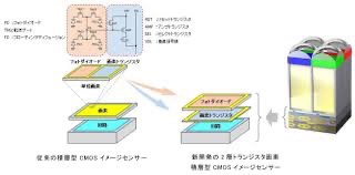
Comparison between 2-layer transistor pixel stack type and conventional type (source: Sony Semiconductor Solutions)
New structure image sensor:
By adopting a new structure, the shooting performance has been doubled and the dynamic range has been expanded.
Noise can also be reduced, improving shooting performance in dark places.
This time, in the new structure:
The “photodiode section responsible for photoelectric conversion” and the “pixel transistor section composed of amplifiers and reset transistors” are formed and stacked on separate substrates.
Conventionally, the PD section and the pixel transistor section were formed on the same wafer.
PD section and pixel transistor section:
The structure was optimized by making the “PD part and pixel transistor part” different wafers.
As a result, if it is a PD part, the “saturation signal amount”, which is the maximum value of electrons that can be accumulated in one pixel, has been increased.

Comparison between 2-layer transistor pixel stack type and conventional type (source: Sony Semiconductor Solutions)
Expanded “saturation signal amount”:
As a result, the dynamic range can be expanded.
With the introduction of the new structure, compared to conventional back-illuminated image sensors, it is possible to secure “twice the saturation signal amount in terms of 1 μm square”.

(Source: Sony Semiconductor Solutions)
Significantly reduced noise when shooting in dark places:
In the pixel transistor section, the size of the amplifier transistor can be increased as the PD section is no longer on the same layer.
This greatly reduces the noise that tends to occur when shooting in dark places.
Nikkei Cross Tech (xTECH)
https://xtech.nikkei.com/atcl/nxt/column/18/00001/06363/
Double layer transistor pixel | Technology | Sony Semiconductor Solutions Group
https://www.sony-semicon.com/ja/technology/mobile/2-layer-pixel.html