大阪市大:GaNとダイヤモンドの直接接合:GaN-on-diamond(動画):
Osaka City Univ: Direct bonding of GaN and diamond: GaN-on-diamond:
大阪市立大学:GaN与金刚石的直接键合:GaN-on-diamond
ーGaN半導体の性能向上に期待ー
大阪市立大学:
研究グループは、
- 次世代半導体材料であるGaNと、
- 究極の半導体とも言われるダイヤモンドを、
常温で直接接合させることに成功した。
大阪市大大学院
東北大学
佐賀大学
アダマンド並木精密宝石ら、研究グループが共同開発した。
GaN-on-diamond:
詳細は国際学術誌「ADVANCED MATERIALS」に掲載された。
GaN-on-diamond構造の実現を目指す研究が進められている。
従来の手法:
従来手法 では、GaNとダイヤモンドの間に中間層が挿入されている。
- その為、放熱性が阻害されたり、
- ダイヤモンドの結晶性が不十分であるなど、
- ダイヤモンドの性能が十分に発揮されない、
上記の課題があったという。
今回の手法:
そうした課題解決を目指し進められた、
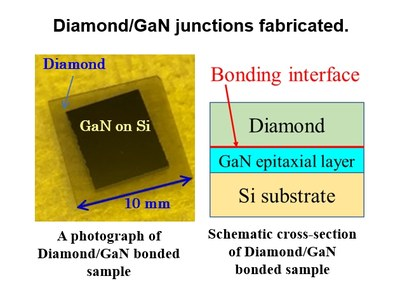
- Si基板上に堆積した、
- 厚さ約1μmのGaN薄層表面に、
- ダイヤモンド基板と表面活性化接合法を用いる。
これで、常温直接接合に成功したという。
常温直接接合の結果:
- Si基板を除去した後、
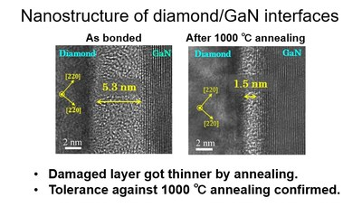
- GaN薄層/ダイヤモンドを窒素雰囲気中で熱処理。
- 1000℃までの熱処理で、接合が維持されていることを確認。
熱処理前後のGaN/ダイヤモンド接合界面の相関関係を調査。
- 1000℃で熱処理後、
- 熱処理前に結晶が壊れていたとしても、
- その領域が減少していることを確認。
今回の成果を踏まえ:
研究グループでは、「接合界面が1000℃の熱処理に耐えること」が判明した。
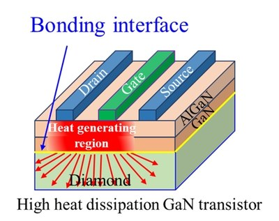
ダイヤモンド接合されたGaN層を加工し、ダイヤモンドの熱伝導性を、最大限に発揮させる。
TECH+
https://news.mynavi.jp/article/20210910-1969716/
GaN-on-diamond semiconductor material that can take the heat – 1,000℃ to be exact
Summary
Researchers
succeed in the direct bonding of diamond and gallium nitride (GaN) at room temperature and demonstrate that
the bond can withstand heat treatments of 1,000℃, making it ideal for the high temperature fabrication process of GaN-based devices.
GaN-on-diamond semiconductor material will allow for the next generation of high power, high frequency devices.
Research outline
The need for more powerful electronic devices in today’s society
is curtailed by our ability to produce highly conductive semiconductors that can withstand the harsh, high temperature fabrication processes of high-powered devices.
Gallium nitride (GaN)-on-diamond
shows promise as a next-generation semiconductor material due to the wide band gap of both materials, allowing for high conductivity, and diamond’s high thermal conductivity, positioning it as a superior heat-spreading substrate.
There have been attempts at creating a GaN-on-diamond structure by combining the two components with some form of transition or adhesion layer,
but in both cases the additional layer significantly interfered with diamond’s thermal conductivity – defeating a key advantage of the GaN-diamond combination.
There is thus a need for a technology that can directly integrate diamond and GaN,” states Jianbo Liang, Associate Professor of the Graduate School of Engineering, Osaka City University (OCU),
and first author of the study, “However, due to large differences in their crystal structures and lattice constants, direct diamond growth on GaN and vice versa is impossible.”
As reported this week in the journal ADVANCED MATERIALS,
Liang, Shigekawa and their colleagues from Tohoku University,
Saga University,
and Adamant Namiki Precision Jewel. Co., Ltd,use the SAB method to successfully bond GaN and diamond, and demonstrate that the bonding is stable even when heated to 1,000℃.
SAB creates highly strong bonds between different materials at room temperature
by atomically cleaning and activating the bonding surfaces to react when brought into contact with each other.
Osaka City University