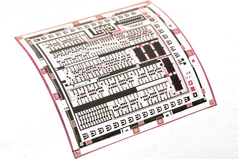
东丽:在薄膜上形成半导体电路:
-确立碳纳米管涂层技术-
东丽:
使用独特的高性能半导体 CNT 复合物,
半导体电路被涂敷并形成在薄膜上。
确立了突破性的技术。
在玻璃基板上制造半导体:
两年前,我们成功地在玻璃基板上制造了涂层半导体。
它具有世界上最高水平的性能,并得到了改进。
在薄膜上制造半导体:
通过改进每种材料,使工艺变得更冷、更短,并且抑制了薄膜的膨胀和收缩。它是
吸引 RFID 和传感器。
目标是将销售额扩大到100亿日元。
半导体碳纳米管复合物:
一种不粘附在 CNT 表面上的半导体聚合物。
在保持 CNT 导电性的同时
半导体聚合物可以分散均匀,
半导体是通过应用分散体制成的。
半导体中的空穴和迁移率:
半导体中的空穴迁移率
涂层类型达到世界最高水平,
它已达到每伏秒 182 ㎠。
东丽工程:
应用形状跟随高精度喷墨技术。
可以形成各种半导体电路和存储器。
可以通过印刷处理小批量生产。
与硅半导体相比
因为制造工艺简单
还可以预期成本降低。
新开关
Toray Develops Semiconductor Circuits on Film by all Printing Process
Demonstrates wireless operations of RFIDs and sensors
semiconductor circuit printing on films,
Toray’s technology
offers considerable design flexibility and can cater to small-lot production needs.The company plans to
initially start with small-lot, short-range wireless communication applications that take advantage of this feature.It will thereafter broaden applications
as it builds up results and cuts costs.Toray plans to exhibit this technology
at nano tech 2022, an international nanotechnology exhibition and conference at Tokyo Big Sight from January 26 through 28, 2022.
Latest News | Toray Industries, Inc.
https://www.toray.com/global/news/details/20220114175355.html