2nm下一代晶體管:開發低接觸電阻技術!
ーAIST:實現2nm邏輯半導體的更高性能ー
ー日台:打造2nm Si/Ge異質通道整合平台ー
AIST
東京都立大學
該研究小組開發了一種“可提高 n 型 MoS2 晶體管性能的低接觸電阻技術”。
它可以有助於提高下一代邏輯半導體的性能。
超過 2nm 的下一代晶體管:
作為通道的半導體材料,
MoS2(二硫化鉬)是一種具有二維晶體結構的TMDC(過渡金屬二硫化物)材料,引起了人們的關注。
TMDC材料MoS2的缺點:
MoS2是
“與金屬電極的接觸面接觸電阻高”
這是“抑制驅動電流並阻礙性能提升的一個因素”。
如何消除高接觸電阻:
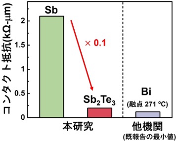
若採用“Bi(鉍)、Sb(銻)等半金屬”作為接觸材料,則可大大降低。
但,
Bi(鉍)和Sb(銻)存在“熔點低,熱穩定性差”的問題。
研究組:
我們充分利用了“適合量產的濺射法”。
通過在單層 MoS2 上形成 Sb2Te3(三碲化二銻)薄膜解決了這個問題。
結果,大大降低了晶體管的接觸電阻。
什麼是 Sb2Te3:
眾所周知,它具有 620°C 的高熔點,同時具有與半金屬相似的特性。
我們在保持高耐熱性的同時實現了低接觸電阻。
未來的 CMOS 製造:
我們的目標是通過串聯連接 n 型和 p 型 TMDC 晶體管來製造 CMOS。
我們將繼續開發適用於 p 型 TMDC 的其他接觸材料。
-電腦手錶
https://pc.watch.impress.co.jp/docs/news/1478116.html
AIST:2nm代新結構晶體管開發
– 堆疊式 Si/Ge 異質溝道互補場效應晶體管顯著提高集成度 –
觀點
日台半導體研發基地:打造2nm世代Si/Ge異質通道整合平台
Si n型場效應管/Ge p型場效應管:實現垂直堆疊晶體管新結構
向實現能夠以低功耗進行高速信息處理的大規模集成電路邁出新的一步
https://www.aist.go.jp/aist_j/press_release/pr2020/pr20201208/pr20201208.html
Transistor de nouvelle génération 2 nm : technologie développée à faible résistance de contact !
ーAIST : Réalisation de performances supérieures dans les semi-conducteurs logiques 2nmー
ーJapon-Taïwan : construire une plate-forme d’intégration de canaux hétérogènes Si/Ge 2nmー
AIST
Université métropolitaine de Tokyo
Le groupe de recherche a développé une “technologie à faible résistance de contact qui améliore les performances des transistors MoS de type n”.
Il peut contribuer à améliorer les performances des semi-conducteurs logiques de nouvelle génération.
Transistors de nouvelle génération au-delà de 2 nm :
En tant que matériau semi-conducteur pour le canal,
MoS2 (disulfure de molybdène), un matériau TMDC (dichalcogénure de métal de transition) avec une structure cristalline bidimensionnelle, a attiré l’attention.
Faiblesses du matériau TMDC MoS2 :
MoS2 est
“Haute résistance de contact à la surface de contact avec l’électrode métallique”
C’était “un facteur qui supprime le courant d’entraînement et entrave l’amélioration des performances”.
Comment éliminer la résistance de contact élevée :
Si “des semi-métaux tels que Bi (bismuth) et Sb (antimoine)” sont utilisés comme matériaux de contact, cela peut être considérablement réduit.
mais,
Bi (bismuth) et Sb (antimoine) avaient un problème de “faible stabilité thermique en raison d’un point de fusion bas”.
Groupe de recherche:
Nous avons pleinement utilisé la “méthode de pulvérisation adaptée à la production de masse”.
Le problème a été résolu en formant un film de Sb2Te3 (tritellurure de diantimoine) sur une seule couche de MoS2.
En conséquence, la résistance de contact du transistor est fortement réduite.
Qu’est-ce que Sb2Te3 :
Il est connu pour avoir un point de fusion élevé de 620°C, tout en ayant des propriétés similaires à celles des semi-métaux.
Nous avons obtenu une faible résistance de contact tout en maintenant une résistance élevée à la chaleur.
Fabrication du futur CMOS :
Notre objectif est de fabriquer du CMOS en connectant en série des transistors TMDC de type n et de type p.
Nous continuerons à développer d’autres matériaux de contact adaptés aux TMDC de type p.
-Montre PC
AIST : Développement d’une nouvelle structure de transistor pour la génération 2nm
– Amélioration significative de l’intégration par des transistors à effet de champ complémentaires à canaux hétérogènes Si/Ge empilés –
indiquer
Base de R&D Japon-Taiwan sur les semi-conducteurs : création d’une plate-forme d’intégration de canaux hétérogènes Si/Ge pour la génération 2 nm
Transistor à effet de champ de type Si n/transistor à effet de champ de type Ge p : réalisation d’une nouvelle structure de transistors empilés verticalement
Une nouvelle étape vers la réalisation de circuits intégrés à grande échelle capables de traiter l’information à grande vitesse avec une faible consommation d’énergie
2-nm-Transistor der nächsten Generation: Entwickelte Technologie mit niedrigem Kontaktwiderstand!
ーAIST: Realisierung einer höheren Leistung in 2-nm-Logikhalbleiternー
ーJapan-Taiwan: Aufbau einer heterogenen 2-nm-Si/Ge-Kanalintegrationsplattformー
AIST
Tokyo Metropolitan University
Die Forschungsgruppe hat eine „Technologie mit niedrigem Kontaktwiderstand entwickelt, die die Leistung von MoS-Transistoren vom n-Typ verbessert“.
Es kann dazu beitragen, die Leistung von Logikhalbleitern der nächsten Generation zu verbessern.
Transistoren der nächsten Generation jenseits von 2 nm:
Als Halbleitermaterial für den Kanal
MoS2 (Molybdändisulfid), ein TMDC-Material (Übergangsmetalldichalkogenid) mit einer zweidimensionalen Kristallstruktur, hat Aufmerksamkeit erregt.
Schwächen des TMDC-Materials MoS2:
MoS2 ist
„Hoher Übergangswiderstand an der Kontaktfläche zur Metallelektrode“
Es war “ein Faktor, der den Antriebsstrom unterdrückt und die Leistungsverbesserung behindert”.
So beseitigen Sie hohe Kontaktwiderstände:
Werden als Kontaktwerkstoffe „Halbmetalle wie Bi (Bismut) und Sb (Antimon)“ verwendet, lässt sie sich stark reduzieren.
Aber,
Bi (Bismut) und Sb (Antimon) hatten ein Problem der “geringen thermischen Stabilität aufgrund des niedrigen Schmelzpunkts”.
Forschungsgruppe:
Wir haben das „massentaugliche Sputterverfahren“ voll ausgeschöpft.
Das Problem wurde gelöst, indem ein Film aus Sb2Te3 (Diantimontritellurid) auf einer einzelnen Schicht aus MoS2 gebildet wurde.
Dadurch wird der Kontaktwiderstand des Transistors stark reduziert.
Was ist Sb2Te3:
Es ist bekannt, dass es einen hohen Schmelzpunkt von 620°C hat, während es ähnliche Eigenschaften wie Halbmetalle hat.
Wir erreichten einen niedrigen Kontaktwiderstand bei gleichzeitig hoher Hitzebeständigkeit.
Zukünftige CMOS-Fertigung:
Unser Ziel ist es, CMOS herzustellen, indem wir TMDC-Transistoren vom n-Typ und p-Typ in Reihe schalten.
Wir werden weiterhin andere Kontaktmaterialien entwickeln, die für TMDCs vom p-Typ geeignet sind.
-PC-Uhr
AIST: Entwicklung eines Transistors mit neuer Struktur für die 2-nm-Generation
– Signifikante Verbesserung der Integration durch gestapelte Si/Ge-Feldeffekttransistoren mit heterogenen Kanälen –
Punkt
Japan-Taiwan-Halbleiter-F&E-Basis: Aufbau einer heterogenen Si/Ge-Kanal-Integrationsplattform für die 2-nm-Generation
Si-n-Typ-Feldeffekttransistor/Ge-p-Typ-Feldeffekttransistor: Erreichen einer neuen Struktur von vertikal gestapelten Transistoren
Ein neuer Schritt zur Realisierung hochintegrierter Schaltkreise, die zur Hochgeschwindigkeits-Informationsverarbeitung bei geringem Stromverbrauch fähig sind
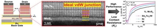
Sb2Te3/MoS2 Van der Waals Junctions with High Thermal Stability and Low Contact Resistance
– X-MOL
Two-dimensional transition metal
dichalcogenides (TMDCs)
demonstrate great potential in nanoelectronics devices owing to their high carrier mobility in the atomically thin channel regime.
However, high contact resistance between source/drain electrodes and TMDC channels
hinders the TMDCs applications in the very-large-scale integration (VLSI) field.
Here, this work reports
atomically aligned van der Waals (vdW) junction fabrications through thermal-induced crystallization of layered Sb2Te3electrodes on monolayer MoS2 using VLSI-compatible physical vapor deposition and annealing processes.
Due to Fermi-level unpinning with a small band offset between Sb2Te3 and MoS2 and small density of state of Sb2Te3,
better device performance is demonstrated on MoS2 MOSFETs with Sb2Te3/W contact than that of Sb/W contact.
Moreover,
the ideal vdW junctions are found to demonstrate extreme high-thermal robustness.
No intermixing at the Sb2Te3/MoS2 interface or crystallinity degradation of Sb2Te3 is observed
after 450 °C annealing, leading to higher thermal stability than its Sb counterpart.
Sb2Te3 is a promising candidate as an n-type contact material for TMDC-based devices such as MoS2, MoSe2, and WS2 in future VLSI electronics and various other applications.