三星:3nm良率沒有提升:
-2022年上半年將難以提供-
三星3nm工藝:
3nm工藝的月產量為30,000至35,000片晶圓(300mm晶圓)。
我們已經收到了來自多個客戶的訂單,例如 HPC 和智能手機處理器。
產量沒有提高:
2021年,三星的目標是“領先台積電實現3nm工藝的量產”。
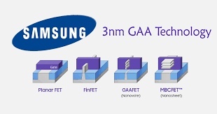
全方位門 (GAA) 結構:
然而,三星的GAA並沒有像預期的那樣站得住腳。
看來3nm的良率很差,舉步維艱。
台積電計劃從 2nm 開始採用 GAA
預計耗時近一年:
三星的 3nm 工藝良率需要將近一年的時間才能穩定下來。
按照三星提出的 2021 年時間表,很難實現量產。
技術 +
https://news.mynavi.jp/techplus/article/20220426-2330741/
Samsung : Aucune amélioration du rendement de 3 nm :
-Il sera difficile de fournir au premier semestre 2022-
Processus Samsung 3 nm :
La production mensuelle du procédé 3nm est de 30 000 à 35 000 wafers (wafer de 300 mm).
Nous avons déjà reçu des commandes de plusieurs clients tels que des processeurs HPC et des smartphones.
Le rendement ne s’améliore pas :
En 2021, Samsung visait à “réaliser la production de masse du processus 3 nm avant TSMC”.
Structure de la porte tout autour (GAA) :
Cependant, le GAA de Samsung ne résiste pas comme prévu.
Il semble que le rendement de 3 nm soit médiocre et qu’il se débatte.
TSMC prévoit d’adopter GAA à partir de 2 nm
Devrait prendre près d’un an :Il faudra près d’un an pour que le rendement du processus 3 nm de Samsung se stabilise.
Il est difficile de parvenir à une production de masse selon le calendrier présenté par Samsung en 2021.
TECH +
Samsung: Keine Ertragsverbesserung von 3nm:
-Bereitstellung im ersten Halbjahr 2022 schwierig-
Samsung 3nm-Prozess:
Die monatliche Produktion des 3-nm-Prozesses beträgt 30.000 bis 35.000 Wafer (300-mm-Wafer).
Wir haben bereits Bestellungen von mehreren Kunden wie HPC und Smartphone-Prozessoren erhalten.
Ertrag verbessert sich nicht:
Im Jahr 2021 strebte Samsung an, „die Massenproduktion des 3-nm-Prozesses vor TSMC zu erreichen“.
Gate All Around (GAA) Struktur:
Samsungs GAA hält sich jedoch nicht wie erwartet.
Es scheint, dass die Ausbeute von 3nm schlecht ist und es Probleme gibt.
TSMC plant, GAA von 2nm zu übernehmen
Voraussichtlich fast ein Jahr dauern:Es wird fast ein Jahr dauern, bis sich die Ausbeute des 3-nm-Prozesses von Samsung stabilisiert hat.
Es ist schwierig, die Massenproduktion nach dem von Samsung vorgelegten Zeitplan im Jahr 2021 zu erreichen.
TECH+
TSMC, ‘3-nano’ confidence… Focus on Samsung’s ‘Foundry’ Strategy
Samsung Electronics
started mass production of 3 nanometers ahead of TSMC,but it is predicted that competition for yield or customer acquisition
will not be easy with those who are following quickly, so attention is focused on strategies for making a breakthrough in the future.
According to foreign media such as Taiwan’s Digitimes on the 18th,
TSMC is ready
to mass-produce 3-nano process chips in the second half of this year.It is expected that the 3nm process will be able to process 30,000 to 35,000 wafers per month only at the beginning of mass production.
Samsung, ahead of TSMC last year,
set the goal of succeeding in mass production of the 3nm process within the first half of this year and is implementing it,
but problems such as yield and securing customers can act as decisive variables in 3nm competition.
Samsung’s 3-nano gate all-around (GAA) process was evaluated
as the basis for its technological prowess to catch up with TSMC and raised expectations. The industry’s view is that it doesn’t mean much.
Samsung Electronics’ new head of semiconductor (DS) division,
Kye-Hyun Kye,
is leading the way to improve the organizational structure that enables more efficient work, while at the same time communicating between employees.Internet New Daily
https://biz.newdaily.co.kr/site/data/html/2022/04/17/2022041700088.html