
LSI 晶片和 FPGA:超越量子計算機
-東京理科大學開發的“LSI系統”
-以更低的功耗使組合最佳化問題更快
我們將為您提供在 News Switch 上發表的文章摘要。
Tokyo University of Science: Professor Takayuki Kawahara
We have developed an LSI system with computational power exceeding that of a quantum computer.
1. Uses CMOS with a circuit line width of 22 nm.
2. Scalable at 4096 bits

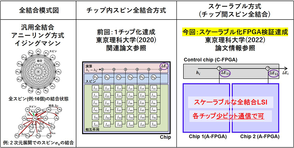
ully coupled Ising LSI system:
Expanded functionality by operating multiple chips in parallel.
Large-scale calculations are possible without using cloud services for large equipment.
Professor Kawahara and his colleagues developed the scalable, fully connected “Ising LSI system.”
Distributed processing of calculation functions:
Expand functionality by connecting multiple LSI chips.
1. Arithmetic functions that were previously contained within a single chip are now distributed over multiple chips.
2. Connect to multiple general-purpose CMOS separately.
We proved with an actual device that the calculation function can be expanded to multiple chips.
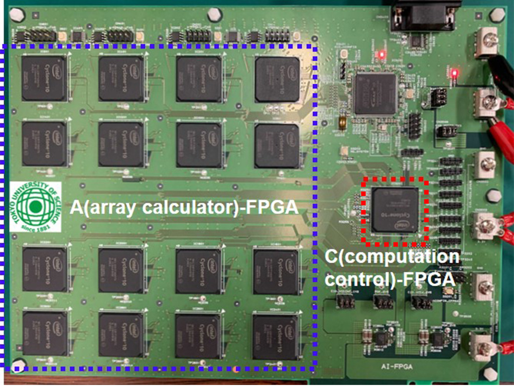
LSI chip and FPGA:
This time, it was fabricated using 22 nanometer CMOS.
1. Equipped with 36 calculation LSI chips.
2. Combines one control FPGA (= rewritable arithmetic circuit).
4096 bit large scale system:
3. We prototyped a large-scale system with 4096 bits.
4. This exceeds current gate-based quantum computers.
We have increased the degree of integration by adopting a new mounting method that can reduce the number of chips by half.
“Vertex covering problem” with 4096 vertices:
One of the combinatorial optimization problems.
We confirmed that the ‘vertex covering problem of 4096 vertices’ can be easily solved.
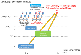
The goal is to surpass quantum computers:
By around 2030, the number of bits will be increased to 2 megabits (mega is 1 million).
The goal is to achieve computing power that exceeds that of quantum computers, which will be achieved around 2050.
Difficulties with superconducting/quantum computers:
Quantum computers are good at solving combinatorial optimization problems.
The superconducting method requires large-scale equipment to cool the material to extremely low temperatures.
Advantages of silicon semiconductor/LSI systems
In contrast, it has become possible to perform the same calculations using existing silicon semiconductor LSIs.
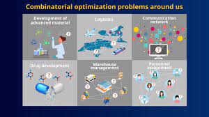
It can be easily used in the field, such as drug discovery, materials development, logistics, finance, and marketing.
Scalable fully coupled Ising semiconductor system
We bring you a summary of articles published by Tokyo University of Science.
Research summary and points:
We have developed a technology to solve combinatorial optimization problems quickly and with low power consumption.
Annealing method that does not use quantum effects:
Developed an annealing method that does not use quantum effects, which is one of the quantum inspired technologies.
This time, we have achieved a large-scale fully coupled Ising semiconductor system using an annealing method.
We verified the “principle of scalable technology using LSI chips.”
By increasing the capacity with LSI chips, it is possible to quickly achieve the performance required for combinatorial optimization problems.
Utilizing the properties of ferromagnetic spin:
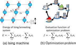
Solving combinatorial optimization problems using the brute force method requires enormous computational resources.
‘The Ising model method’ solves this problem.
1. At high temperatures, the spins are in random directions.
At high temperatures, the spins of a ferromagnetic material with no magnetization become randomly oriented.
2. At low temperatures, the spin directions align
Lowering the temperature follows the ‘interconnection’ without having to try all possibilities.
In other words, the spin directions naturally align and magnetization occurs.
This property is applied to solving combinatorial optimization problems.
This quantum inspired technology:
In fact, it is an important technological field in which Japan excels.
The ferromagnetic model should not be used as is.
1. ‘Fully coupled type that couples all spins’.
2. Can be realized with a small mounting area (= in the case of adjacent coupling type, the square of the total number of bonded spins is required)
3. Highly versatile and can solve a wide range of problems (= simple conversion process to solve problems)

Equipped with 512 fully connected spins:
In 2020, a new chip architecture was realized.
International academic conference IEEE: SAMI 2020
Equipped with 512 fully coupled spins.
Announced AI chip using fully coupled semiconductor annealing method.

Details of this research result:
This time, we have devised a method to configure a large-scale Ising LSI system in a scalable manner.
Combines multiple fully coupled Ising LSI chips with an extremely small number of inter-chip connections.
It operates as one fully connected system using an annealing method.
Furthermore, using FPGA, we demonstrated that this method works correctly.
It is the first fully connected type that uses an annealing method to achieve scalability.

Main technologies developed this time:
Devised a method to divide the energy calculation and update the spin.
Using two types of chips,
The energy is divided and calculated using multiple identical first chips.
Add them together using one second chip.
A new way to determine which spin values to update.
The whole works as one fully connected system.
Scalable fully connected system:
The amount of data communication between the first and second chips can be extremely reduced.
This is the first annealing method to achieve a scalable fully connected system.
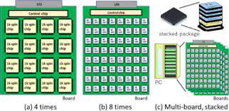
Verification of principle on actual machine:
As the first chip, 16 FPGA chips (A-FPGA),
As the second chip, use one FPGA chip (C-FPGA),
We created a fully coupled annealing processing system board with 384 spins (Figure 2).
We confirmed that it operates as a single fully connected LSI system and can operate with multiple chips with a small amount of communication.
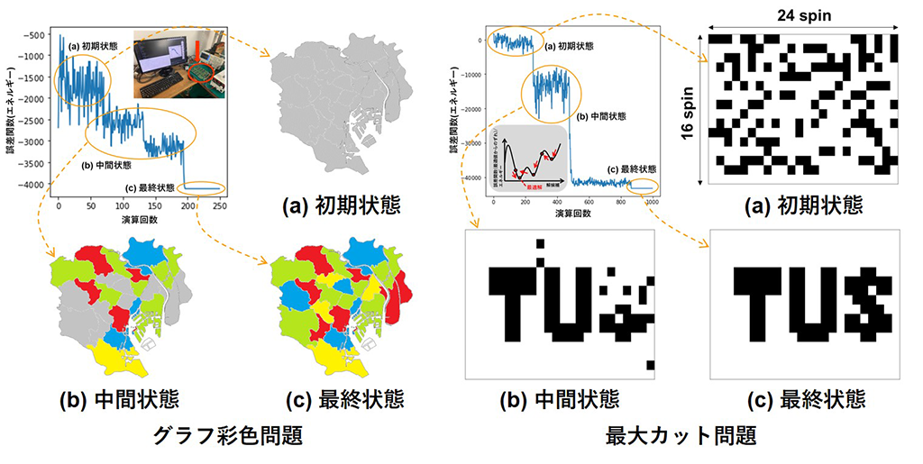
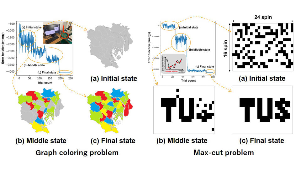
92 node graph coloring problem:
It was shown that the problem could be solved using this actual system.
Maximum cut problem of 384 nodes:
In the maximum cut problem,
On a PC with a 4GHz CPU, we achieved performance that was 584 times faster and 46 times more energy efficient than fully coupled annealing calculations (Figure 3).
Future prospects:
This time, we successfully verified the principle using FPGA.
In the future, we will use custom LSI chips to increase capacity and greatly improve performance and power efficiency.
Quickly achieve the high performance required in the fields of new material development and drug discovery.