Rapidus:成功開發2mm半導體核心技術
・Rapidus和IBM公佈2mm半導體研究成果
・Rapidus將於2025年4月開始製造原型
我們將為您提供日經新聞發表的文章摘要。

Rapidus President Atsuyoshi Koike:
Rapidus and IBM aim to mass-produce cutting-edge semiconductors from next year.
They have jointly developed “core technology to make 2 nm semiconductors operate as designed.”

2 nm semiconductor prototype:
Rapidus will begin prototype production in April 2025.
1. Rapidus has achieved high performance by adopting this technology in its prototypes.
2. Finely control the voltage of the current flowing through the semiconductor.

Overview of this research:
Introduces an “etching process that selectively reduces layers” called SLR (Selective Layer Reductions)
Nanosheets with multi-threshold voltages that can control multiple threshold voltages.
We have succeeded in constructing a GAA (Gate All Around) transistor.

International Electron Devices Meeting (IEDM2024):
IEDM2024 is being held in San Francisco, USA from December 7th to 11th.
1. On December 9th, the two companies announced their research results and their papers were accepted.
2. This is the first time that Rapidus and IBM have “publicly announced the results of their 2nm semiconductor research.”

IBM’s comment:
IBM commented that “the 2nm chip we developed this time cleared strict technical requirements.”
1. 2nm semiconductor elements use a complex structure called GAA (Gate All Around).
2. In order to “prevent electrical leakage from fine circuits,” we have succeeded in “creating an insulating film in a specific layer.”
This 2nm chip can precisely control voltage and can perform complex calculations with less power than before.

Lapidus’ future plans:
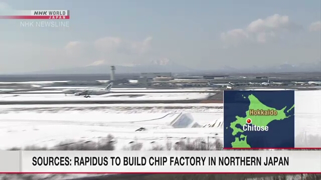
1. From 2025, we will begin prototyping at our Chitose factory in Hokkaido.
2. We aim to start mass production of 2nm semiconductors from 2027.
Lapidus’s Kazuyuki Tomita:
We are currently working with IBM to jointly develop design technology for 2nm semiconductors at IBM’s research center in the US.
We will introduce this technology to Lapidus’ Hokkaido factory next year.
https://www.nikkei.com/article/DGXZQOUC104F10Q4A211C2000000/

Rapidus and IBM move closer to scaling out 2nm chip production
A new chip construction process, called selective layer reductions
helping overcome some of the critical challenges to produce 2nm transistors
Report from IBM Blog

A new chip construction process : called selective layer reductions,
Itis helping overcome some of the critical challenges to produce 2-nanometer transistors and beyond at scale within the decade.
Scientists from IBM and Japanese chipmaker Rapidus have announced that they reached a critical milestone in consistently constructing chips with a 2nm process.
Using two different strategies : for selective nanosheet layer reduction,
they can now build nanosheet gate-all-around transistors with multiple threshold voltages (or multi-Vt),
which allows for chips that can perform complex computations without requiring as much energy.

The group found :
they could do this without the metal gate boundary problems that tend to accompany this construction method.
They present their new research today at the annual IEEE International Electron Devices Meeting (IEDM) in San Francisco.
Three years ago :
IBM Research scientists showed off the world’s first 2 nanometer node chip,
two years ago :
IBM and Rapidus formed a partnership to advance this technology to a place where it would be possible to fabricate 2 nm chips at scale.
With their new results :
the collaboration has brought this effort a crucial step closer to the goal of producing these chips before the end of this decade.

Kazuyuki Tomida : the general manager at Rapidus US, LLC, also mentioned.
Multi-Vt technology is a critical component of our nanosheet architecture.
The joint publication of this technology research paper :
with IBM Research at the IEDM conference represents a substantial milestone for Rapidus.
This achievement reinforces our confidence in realizing our goal of manufacturing in Hokkaido at our advanced IIM foundry.
Dechao Guo : the director of advanced logic technology at IBM Research.also mentioned.
New problems, new solutions:
Producing 2 nm node chips isn’t just a matter of scaling components down, explained Dechao Guo, the director of advanced logic technology at IBM Research.
It also introduces unique challenges compared to the previous industry standard, FinFET transistors.
To achieve our goals for 2nm technology, we need process solutions with nanosheet gate-all-around architecture for multiple threshold voltages.
which enable ultra-low threshold voltages for high-performance computing, and higher threshold voltages for low-power computing.
The team has now demonstrated a vital step toward the first iteration of the next generation of microchips.
https://research.ibm.com/blog/rapidus-ibm-move-closer-to-scaling-out-2-nm-chip-production
